Terahertz plane adsorbing material
A technology of absorbing materials and wave planes, applied in the field of electromagnetic functional materials, to achieve the effects of easy design, good adjustability, and improved performance and efficiency
- Summary
- Abstract
- Description
- Claims
- Application Information
AI Technical Summary
Problems solved by technology
Method used
Image

Examples
Embodiment Construction
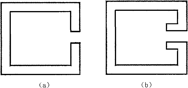
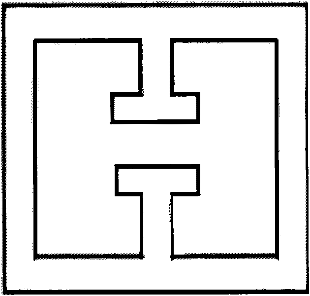
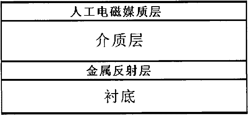
[0020] Design a terahertz wave planar absorbing material with two absorption frequency bands at 0.2-3THz, and the absorption rate reaches more than 85%. Using CST software, build as image 3 The multilayer structure shown includes a substrate, a metal reflective layer, a dielectric layer and an artificial electromagnetic dielectric layer. The structure of the artificial electromagnetic medium unit is as follows: Figure 4 As shown, it is a centrosymmetric figure formed by a metal thin film line with a line width of t (such as Figure 4 shown), including an electric split ring resonator formed by connecting two single-split metal rings in the middle, wherein the openings of the two single-split metal rings are connected to each other to form the opening of the electric split ring resonator; The electric split ring resonator has a single split metal ring with the long sides facing away from the connection. The length of the overall artificial electromagnetic medium unit is b,...
PUM
 Abstract
Description
Claims
Application Information
 - R&D
- Intellectual Property
- Life Sciences
- Materials
- Tech Scout
- Unparalleled Data Quality
- Higher Quality Content
- 60% Fewer Hallucinations
Browse by: Latest US Patents, China's latest patents, Technical Efficacy Thesaurus, Application Domain, Technology Topic, Popular Technical Reports.
© 2025 PatSnap. All rights reserved.Legal|Privacy policy|Modern Slavery Act Transparency Statement|Sitemap|About US| Contact US: help@patsnap.com