Heterojunction bipolar transistor structure with high current gain and processing method thereof
A technology of bipolar transistors and processing methods, which can be applied to circuits, electrical components, semiconductor devices, etc., and can solve problems such as current gain drop
- Summary
- Abstract
- Description
- Claims
- Application Information
AI Technical Summary
Problems solved by technology
Method used
Image


Examples
Embodiment Construction
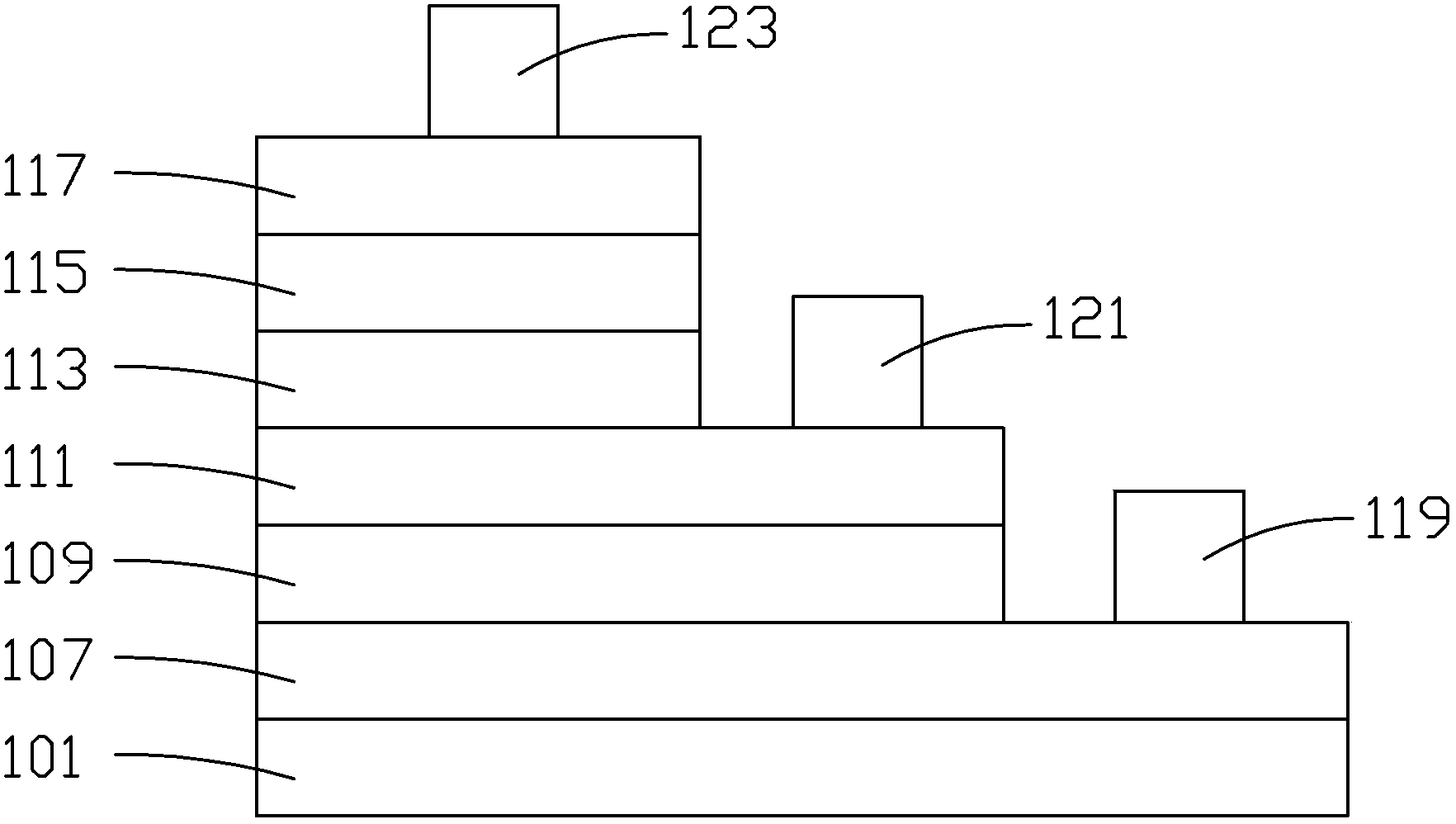
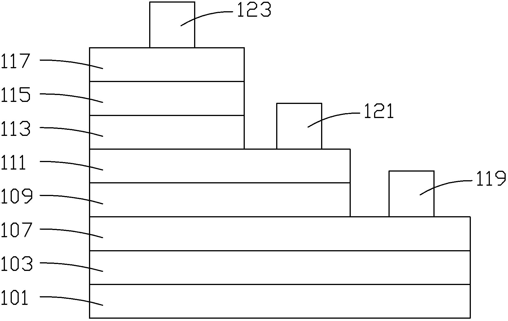
[0029] Figure 4 It is a schematic cross-sectional view of the epitaxial layer structure of the improved structure of the heterojunction bipolar transistor of the present invention, which includes a substrate 201, a p-type doped buffer layer 203, a primary collector layer 207, a collector layer 209, and a The base layer 211, an emitter layer 213, a collector electrode 219, a base electrode 221, and an emitter electrode 223.
[0030] In the structure of the present invention, the substrate 201 may generally be a semi-insulating gallium arsenide (GaAs) substrate. The p-type doped buffer layer 203 is formed on the substrate 201 by epitaxial growth technology. Existing epitaxial growth technologies include Molecular Beam Epitaxy (MBE) technology or Metal-organic Chemical Vapor Deposition (MOCVD) technology. The p-type doped buffer layer material can be gallium arsenide (GaAs), aluminum gallium arsenide (AlGaAs), indium gallium phosphide (InGaP), indium aluminum phosphide (InAlP), in...
PUM
 Abstract
Description
Claims
Application Information
 - R&D
- Intellectual Property
- Life Sciences
- Materials
- Tech Scout
- Unparalleled Data Quality
- Higher Quality Content
- 60% Fewer Hallucinations
Browse by: Latest US Patents, China's latest patents, Technical Efficacy Thesaurus, Application Domain, Technology Topic, Popular Technical Reports.
© 2025 PatSnap. All rights reserved.Legal|Privacy policy|Modern Slavery Act Transparency Statement|Sitemap|About US| Contact US: help@patsnap.com