Integrated Gan-based sensor and method for simultaneous monitoring of solution temperature and pH
A sensor and integrated technology, applied in thermometers, thermometers and instruments with directly sensitive electrical/magnetic components, etc., can solve the problems of high cost and difficult to achieve integration, and achieve improved detection sensitivity, high two-dimensional electronic Effect of Gas Channel Concentration
- Summary
- Abstract
- Description
- Claims
- Application Information
AI Technical Summary
Problems solved by technology
Method used
Image

Examples
Embodiment 1
[0034] This embodiment provides a method for preparing an integrated GaN-based sensor for synchronous monitoring of solution temperature and pH, including the following steps:
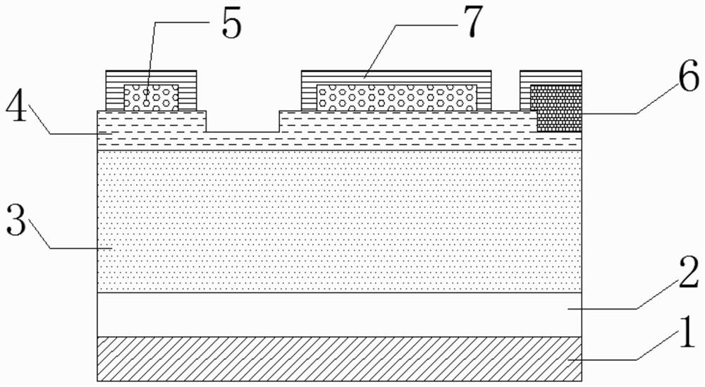
[0035] S1: growing the stress buffer layer 2 and the GaN epitaxial layer 3 sequentially on the upper surface of the substrate layer 1 to obtain a sensor intermediate a; wherein the substrate layer 1 is a Si substrate, a sapphire substrate, a SiC substrate or a GaN substrate Any one of the self-supporting substrates; the stress buffer layer 2 is any one of AlN, AlGaN or GaN, or a combination of any two or more; and according to the difference in specifications, the thickness of the stress buffer layer 2 is between It can be adjusted between 0.01 and 100 μm; the GaN epitaxial layer is an unintentionally doped GaN epitaxial layer, and its dislocation density is 10 7 / cm 3 , the thickness of the GaN epitaxial layer can be adjusted between 0.1 and 100 μm;
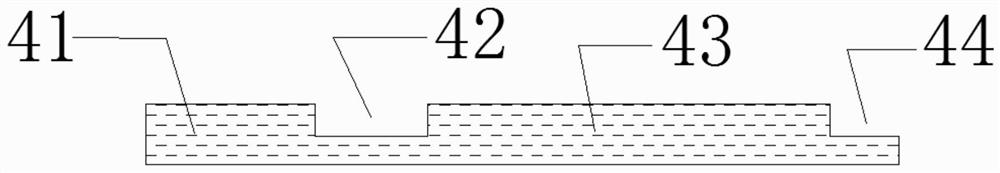
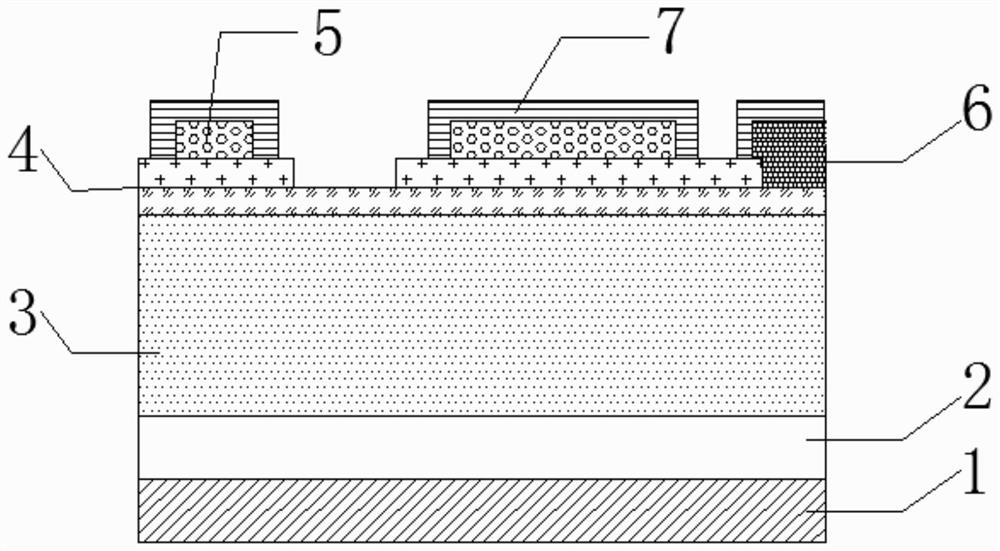
[0036]S2: An AlGaN barrier layer 4 is grown on t...
Embodiment 2
[0039] This embodiment provides a method for preparing an integrated GaN-based sensor for synchronous monitoring of solution temperature and pH, including the following steps:
[0040] I: growing the stress buffer layer and the GaN epitaxial layer sequentially on the upper surface of the substrate layer to obtain a sensor intermediate a; wherein the substrate layer 1 is a Si substrate, a sapphire substrate, a SiC substrate or a GaN self-supporting substrate bottom; the stress buffer layer 2 is any one of AlN, AlGaN or GaN, or any combination of two or more; and according to the difference in specifications, the thickness of the stress buffer layer 2 is 0.01-100 μm can be regulated; the GaN epitaxial layer is an unintentionally doped GaN epitaxial layer, and its dislocation density is 10 8 / cm 3 , the thickness of the GaN epitaxial layer can be adjusted between 0.1 and 100 μm;
[0041] II: On the GaN epitaxial layer of the sensor intermediate a obtained in step I, an AlGaN ba...
PUM
| Property | Measurement | Unit |
|---|---|---|
| thickness | aaaaa | aaaaa |
| thickness | aaaaa | aaaaa |
| thickness | aaaaa | aaaaa |
Abstract
Description
Claims
Application Information
 - R&D
- Intellectual Property
- Life Sciences
- Materials
- Tech Scout
- Unparalleled Data Quality
- Higher Quality Content
- 60% Fewer Hallucinations
Browse by: Latest US Patents, China's latest patents, Technical Efficacy Thesaurus, Application Domain, Technology Topic, Popular Technical Reports.
© 2025 PatSnap. All rights reserved.Legal|Privacy policy|Modern Slavery Act Transparency Statement|Sitemap|About US| Contact US: help@patsnap.com