Circuit board manufacturing method for improving signal transmission precision
A manufacturing method and signal transmission technology, applied in the direction of multi-layer circuit manufacturing, printed circuit manufacturing, printed circuit, etc., can solve the problems of high cost, complex manufacturing process, low speed and precision, etc. The effect of improving work efficiency
- Summary
- Abstract
- Description
- Claims
- Application Information
AI Technical Summary
Problems solved by technology
Method used
Image

Examples
Embodiment 1
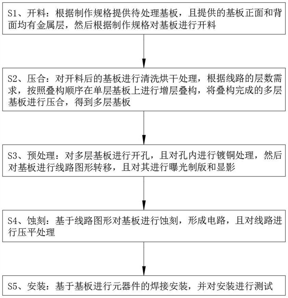
[0029] refer to figure 1 As shown, a method for manufacturing a multilayer circuit board for improving signal transmission accuracy, the method for manufacturing a multilayer circuit board includes the following steps:
[0030] S1. Slicing: Provide the substrate to be processed according to the production specifications, and the provided substrate has a metal layer on the front and back, and then open the substrate according to the production specifications;
[0031] S2. Lamination: Clean and dry the substrate after cutting. According to the number of layers of the circuit, stack the single-layer substrate according to the stacking sequence, and press the laminated multi-layer substrate. to obtain a multi-layer substrate;
[0032] S3. Pretreatment: the multi-layer substrate is opened, and the inside of the hole is copper-plated, and then the circuit pattern is transferred to the substrate, and it is exposed to plate making and development;
[0033] S4. Etching: Etch the subs...
Embodiment 2
[0036] A method for manufacturing a multilayer circuit board for improving signal transmission accuracy, the method for manufacturing the multilayer circuit board comprises the following steps:
[0037] S1. Slicing: Provide the substrate to be processed according to the production specifications, and the provided substrate has a metal layer on the front and back. The metal layer is a copper layer with a thickness of 30-50 microns, and a conductive film is arranged between the metal layer and the substrate. , and then cut the substrate according to the production specifications;
[0038] S2. Lamination: Clean and dry the substrate after cutting. According to the requirements of the number of layers of the circuit, stacking is performed on the single-layer substrate according to the stacking sequence, and PP is arranged between the stacked single-layer substrates. Sheet, the substrate and the PP sheet are stacked in order to form a pre-fixed circuit, the laminated multilayer sub...
Embodiment 3
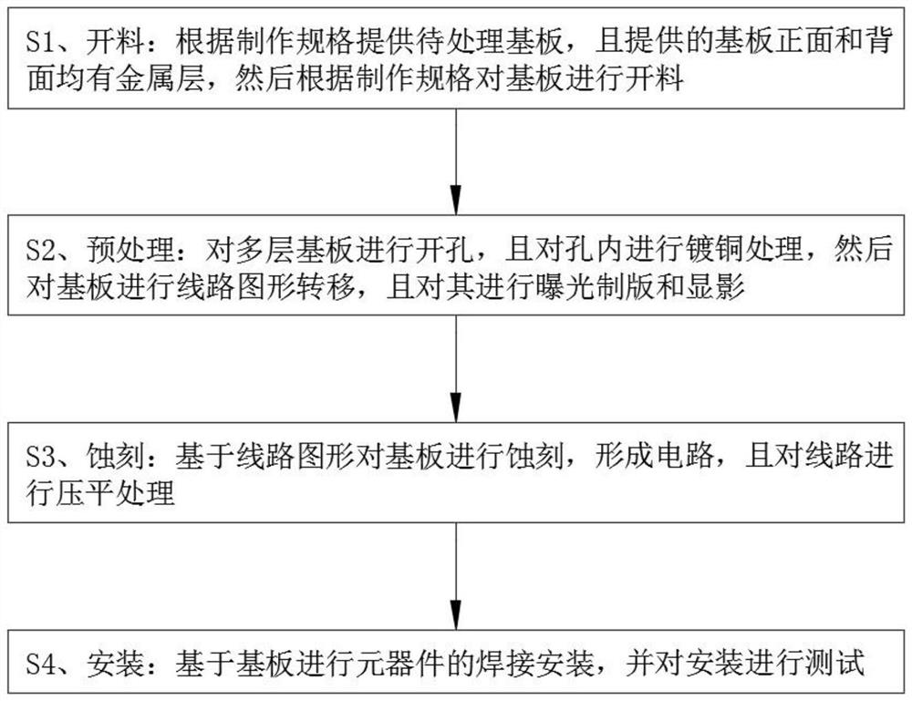
[0043] refer to figure 2 As shown, a method for manufacturing a single-layer circuit board for improving signal transmission accuracy, the method for manufacturing a single-layer circuit board includes the following steps:
[0044] S1. Slicing: Provide the substrate to be processed according to the production specifications, and the provided substrate has a metal layer on the front and back, and then open the substrate according to the production specifications;
[0045] S2, pretreatment: the multi-layer substrate is opened, and the inside of the hole is copper-plated, and then the circuit pattern is transferred to the substrate, and it is exposed to plate making and development;
[0046] S3. Etching: The substrate is etched based on the circuit pattern to form a circuit, and the circuit is flattened;
[0047] S4. Installation: Based on the substrate, the components are welded and installed, and the installation is tested.
PUM
 Abstract
Description
Claims
Application Information
 - R&D
- Intellectual Property
- Life Sciences
- Materials
- Tech Scout
- Unparalleled Data Quality
- Higher Quality Content
- 60% Fewer Hallucinations
Browse by: Latest US Patents, China's latest patents, Technical Efficacy Thesaurus, Application Domain, Technology Topic, Popular Technical Reports.
© 2025 PatSnap. All rights reserved.Legal|Privacy policy|Modern Slavery Act Transparency Statement|Sitemap|About US| Contact US: help@patsnap.com