Method of fabricating semiconductor device
- Summary
- Abstract
- Description
- Claims
- Application Information
AI Technical Summary
Benefits of technology
Problems solved by technology
Method used
Image

Examples
first embodiment
[0066] A first embodiment of the present invention relates to the invention based on the first knowledge as described above.
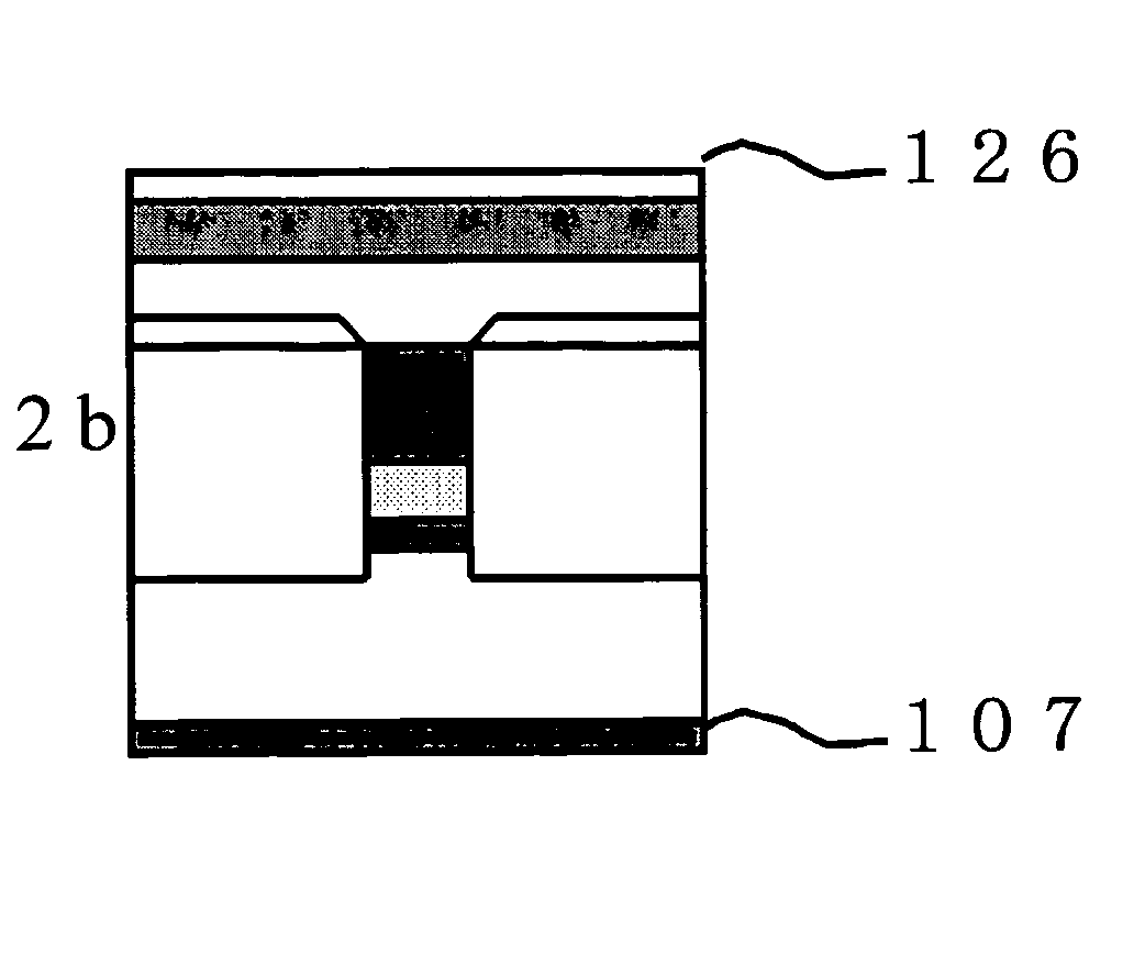
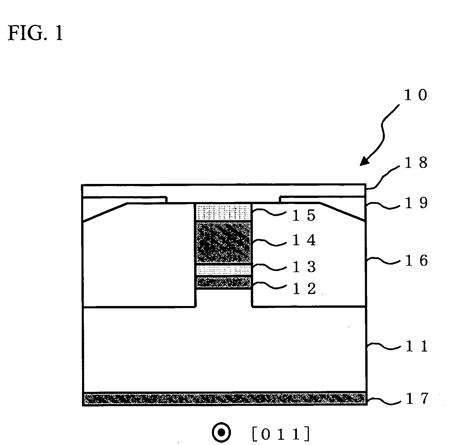
[0067]FIG. 8 is an example of the laser diode of the SIBH (Semi Insulating Buries Hetero) structure in accordance with the first embodiment of the present invention and is a cross-sectional view of the laser diode from the direction of [0-11]. A laser diode 100 includes an n-type (100) InP substrate 101. The n-type (100) InP substrate 101 has an n-side electrode 107 on the backside and the step region on the main surface. The step region extends in the direction of [0-11] in stripes and includes an n-type InGaAsP guide layer 102, an InGaAsP-MQW active layer 103, a p-type InP clad layer 104, and a p-type InGaAs contact layer 105, which are sequentially deposited. The step region is planarized by an Fe-doped high resistant buried layers 106. An SiO2 protective film 109 is provided in the step region with an opening so as to expose the whole plane of the p-type I...
second embodiment
[0078] A second embodiment of the present invention relates to a method of making the height of the step region (100) plane equal to that of the buried layer (100) plane.
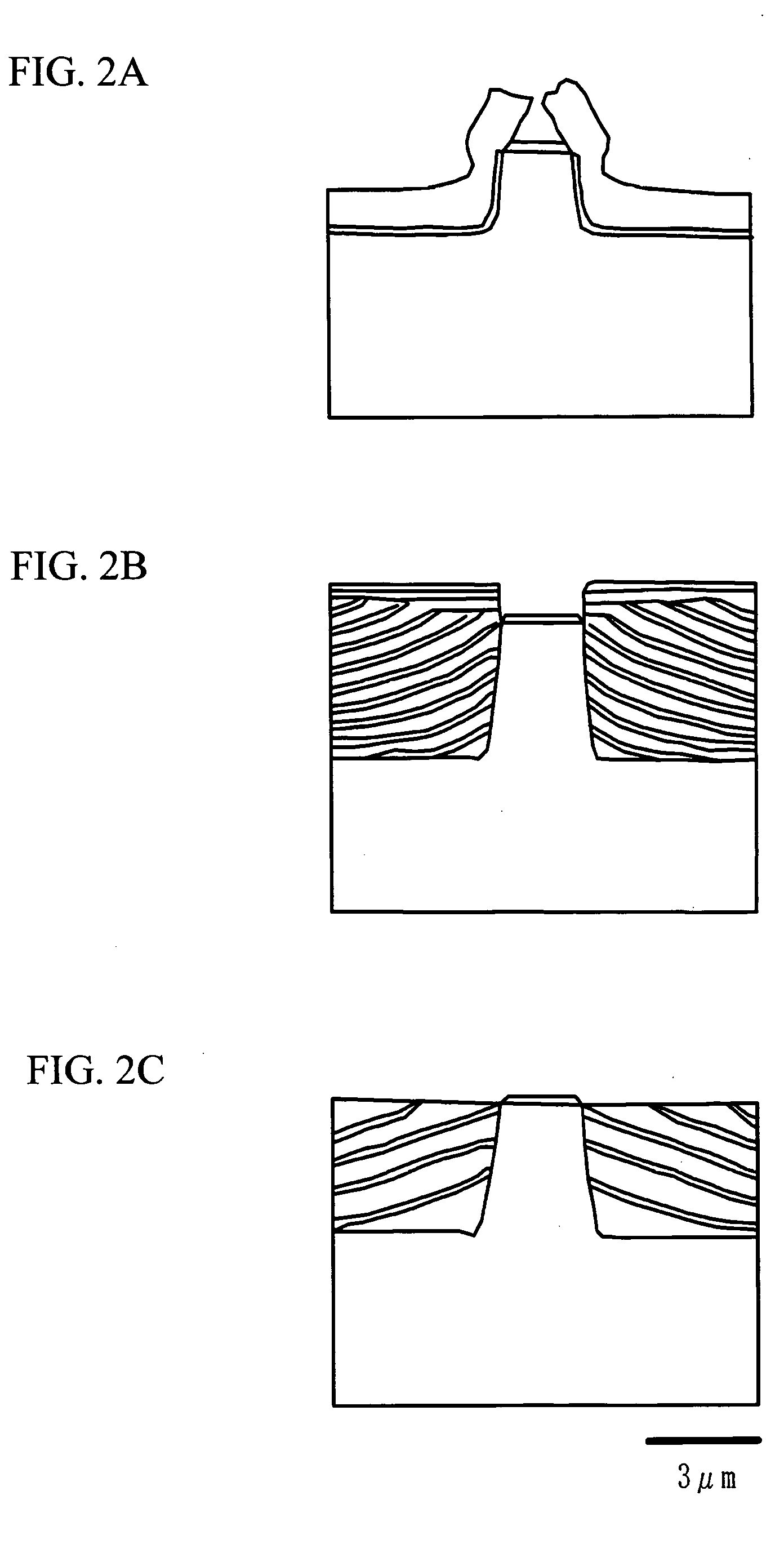
[0079] Referring to FIGS. 11A through 11H, a description will be given of the fabricating processes of the laser diode having the SIPBH structure. First, an n-type InGaAsP layer 115, an InGaAsP layer 116, and a p-type InP layer 117 are sequentially deposited on the main surface of the n-type (100) InP substrate 101 as shown in FIG. 11A. Next, a SiO2 selective growth mask118 is formed in one region of the p-type InP layer 117, with the CVD method, the optical lithography, and HF-based wet etching technique. The SiO2 selective growth mask 118 has a thickness of 0.3 μm and is extending in the direction of [0-11] with the width of 2.5 μm as shown in FIG. 11B.
[0080] In this state, the etching is performed with the RIE method using a mixed gas of ethane, hydrogen, and oxygen to remove the region that is not masked with ...
PUM
 Abstract
Description
Claims
Application Information
 - R&D
- Intellectual Property
- Life Sciences
- Materials
- Tech Scout
- Unparalleled Data Quality
- Higher Quality Content
- 60% Fewer Hallucinations
Browse by: Latest US Patents, China's latest patents, Technical Efficacy Thesaurus, Application Domain, Technology Topic, Popular Technical Reports.
© 2025 PatSnap. All rights reserved.Legal|Privacy policy|Modern Slavery Act Transparency Statement|Sitemap|About US| Contact US: help@patsnap.com