Semiconductor Light Emitting Device
- Summary
- Abstract
- Description
- Claims
- Application Information
AI Technical Summary
Benefits of technology
Problems solved by technology
Method used
Image

Examples
Embodiment Construction
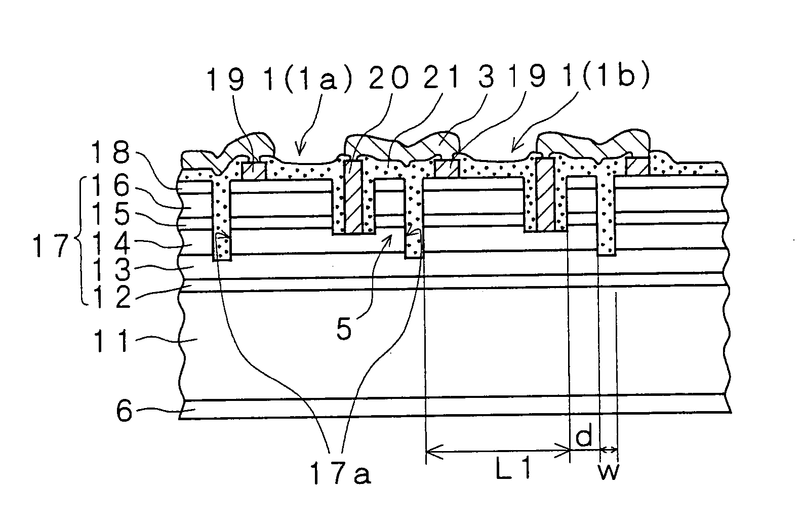
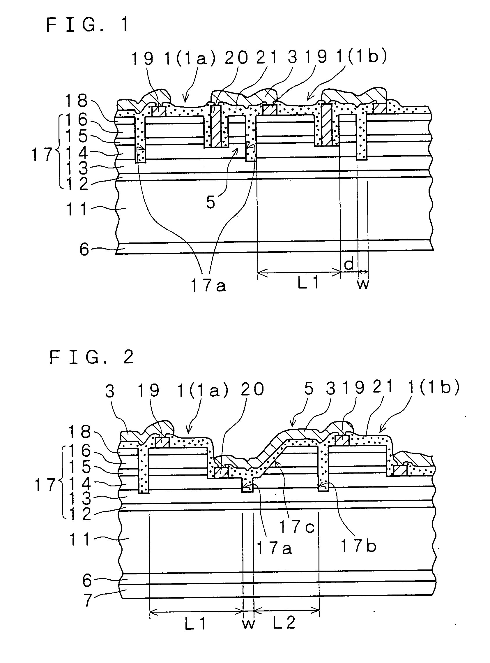
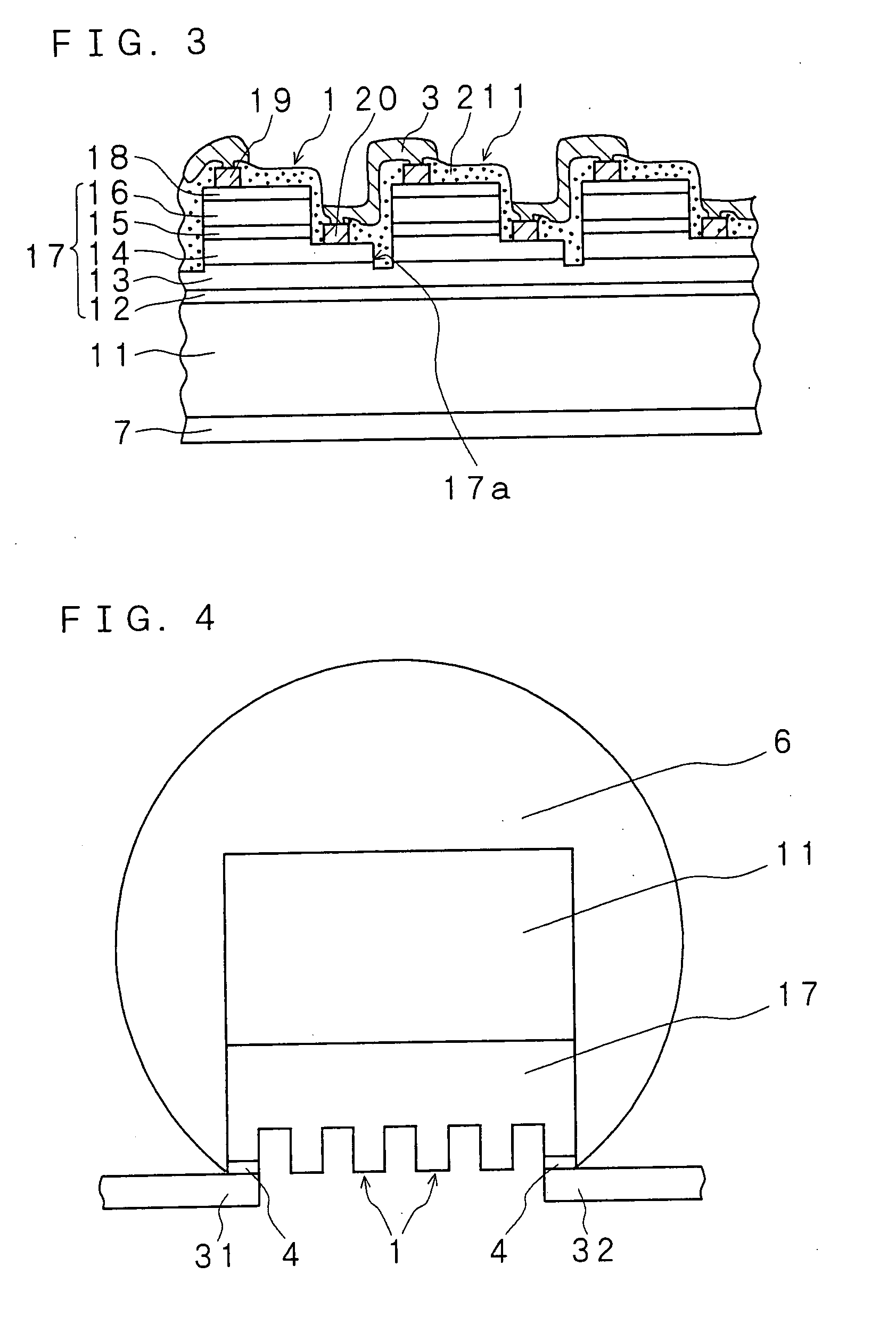
[0041] An explanation will be given below of a semiconductor light emitting device according to the present invention in reference to the drawings. As a cross-sectional view explaining an example is shown in FIG. 1, the semiconductor light emitting device according to the present invention is provided with a semiconductor lamination portion 17 formed on a substrate 11 by laminating semiconductor layers so as to form a light emitting layer and a plurality of light emitting units 1 formed by separating the semiconductor lamination portion 17 electrically into a plurality of units, each of which has a pair of electrodes 19 and 20. Each of the plurality of light emitting units 1 is connected to each other in series and / or parallel through wiring films 3 and provided with a fluorescent layer 6 containing a fluorescent material having an afterglow time of 10 msec or more and 1 sec or less at a light emitting surface side (a surface side radiating light emitted in the light emitting layer)...
PUM
 Abstract
Description
Claims
Application Information
 - R&D
- Intellectual Property
- Life Sciences
- Materials
- Tech Scout
- Unparalleled Data Quality
- Higher Quality Content
- 60% Fewer Hallucinations
Browse by: Latest US Patents, China's latest patents, Technical Efficacy Thesaurus, Application Domain, Technology Topic, Popular Technical Reports.
© 2025 PatSnap. All rights reserved.Legal|Privacy policy|Modern Slavery Act Transparency Statement|Sitemap|About US| Contact US: help@patsnap.com