Method for Manufacturing Photoelectric Converter and Photoelectric Converter
- Summary
- Abstract
- Description
- Claims
- Application Information
AI Technical Summary
Benefits of technology
Problems solved by technology
Method used
Image

Examples
embodiment 1
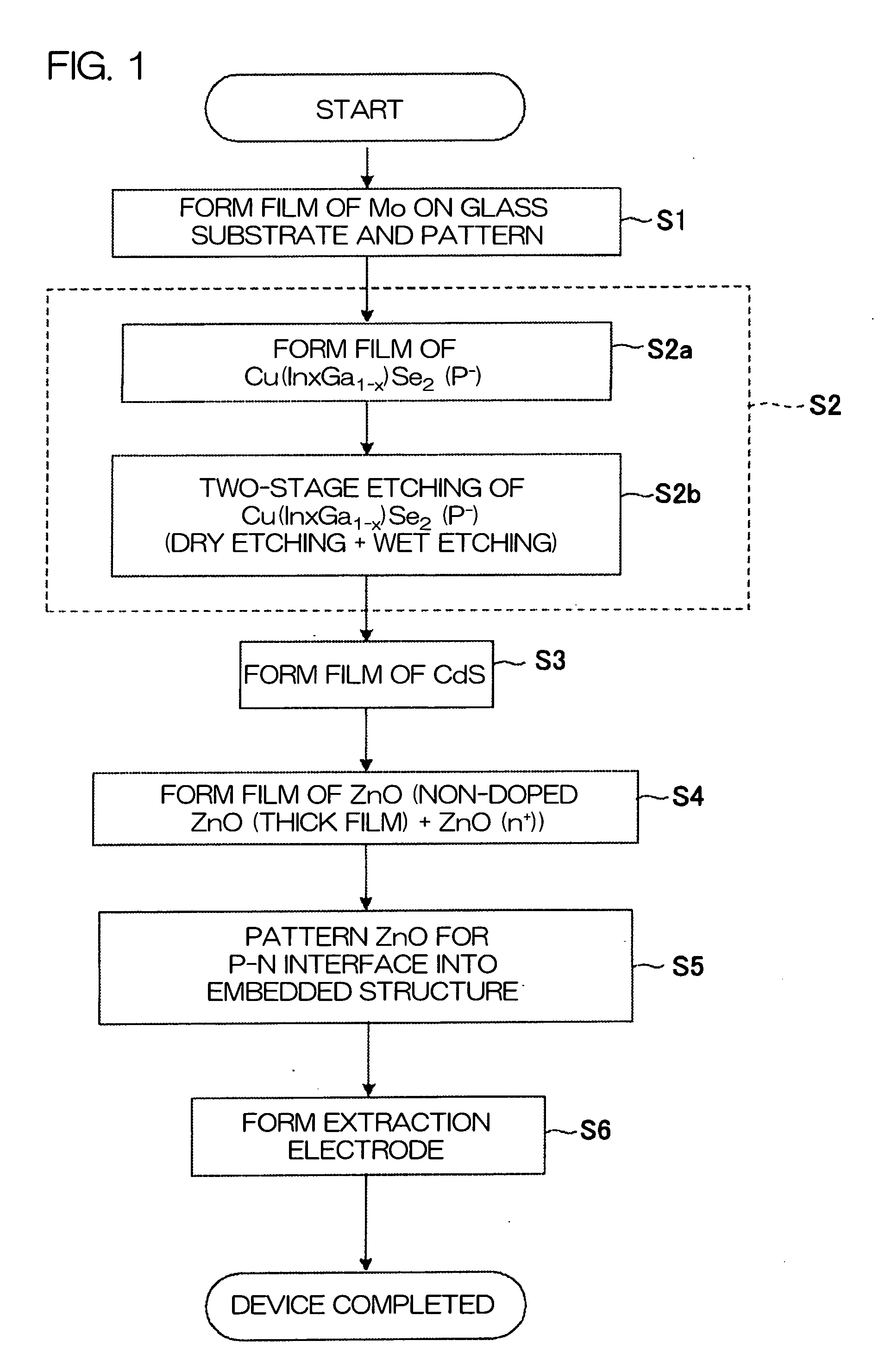
[0063]FIG. 1 is a flow chart showing an outline of a method for manufacturing a photoelectric converter according to the present invention.
[0064]In this manufacturing process, the respective ones of a laminated / formed lower electrode layer, a p-type compound semiconductor thin film (hereinafter referred to as a CIGS thin film) having a chalcopyrite structure serving as a light absorptive layer and a light-transmitting electrode layer (including both of a non-doped portion and a portion doped with an impurity to exhibit an n+ type) are patterned by photolithography for minimizing damages to the crystals of the CIGS thin film.
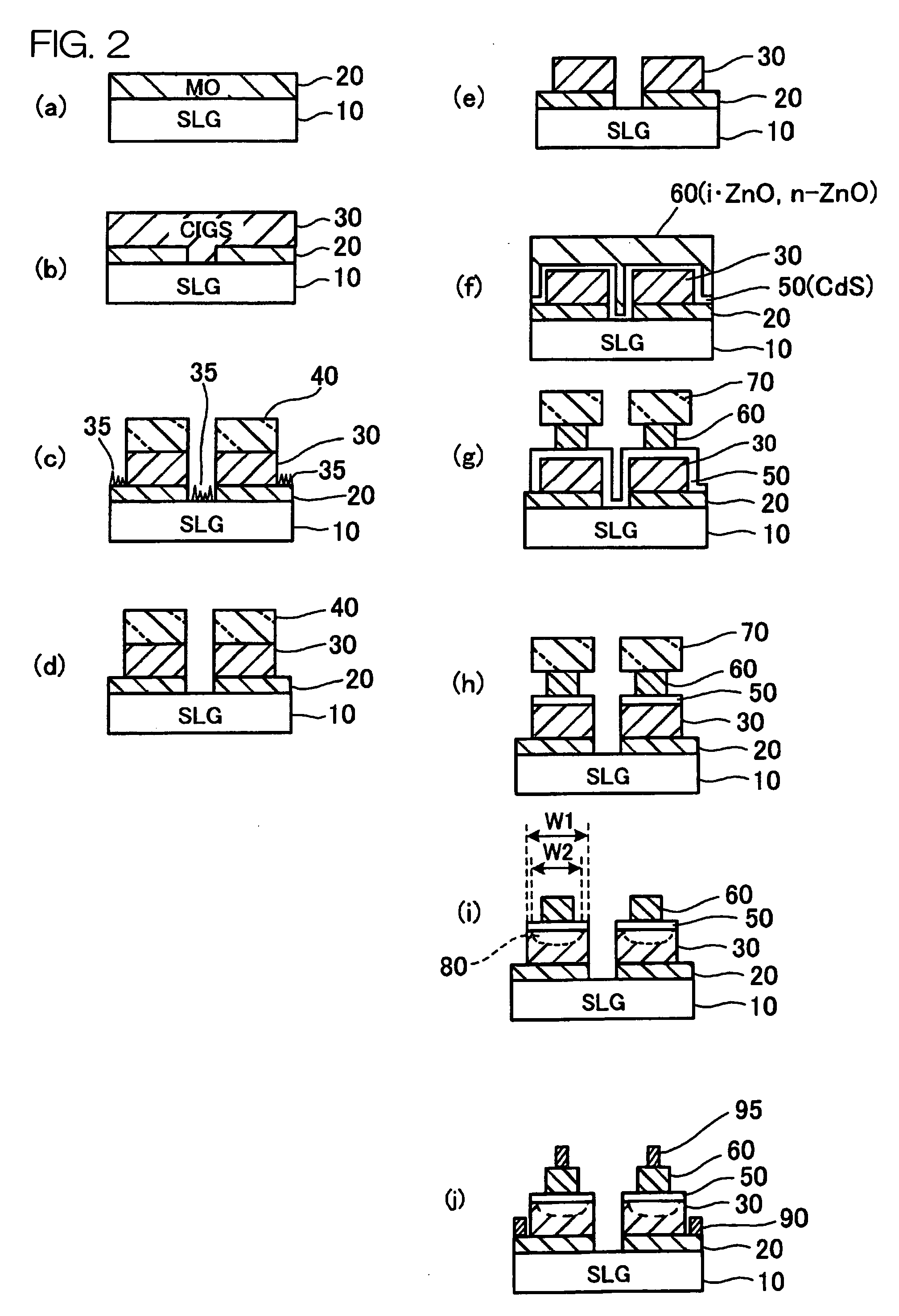
[0065]In the method for manufacturing a photoelectric converter according to the present invention, a Mo (molybdenum) layer for forming a lower electrode is formed by sputtering (about 0.6 μm) on a glass substrate, and thereafter patterned by photolithography (step S1). Thus, an electrically isolated island region of Mo is formed.
[0066]Then, a CIGS thin film is f...
embodiment 2
[0100]In this embodiment, an example of using the photoelectric converter according to the present invention as a photosensor having high sensitivity also in the near infrared region is described.
[0101]FIG. 5 is a diagram showing absorption coefficients of a CIS thin film (also applies to a CIGS thin film) with respect to the wavelengths of light. As is illustrated, it is understood that the CIS thin film (CIGS thin film) has a high sensitivity over a wide range from visible light to near infrared light.
[0102]With attention drawn to this point, a composite image sensor is formed by laminating the photoelectric converter of the present invention made of a compound semiconductor thin film on a silicon substrate formed with MOS transistors or the like in this embodiment.
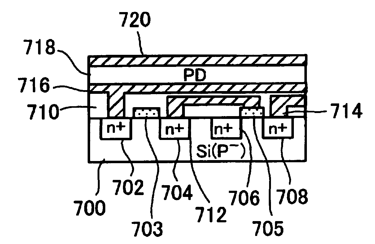
[0103]FIG. 6 is a schematic sectional view of a general CMOS image sensor formed on a silicon substrate. FIG. 7 is a schematic sectional view of the composite image sensor according to the present invention formed by la...
PUM
 Abstract
Description
Claims
Application Information
 - R&D
- Intellectual Property
- Life Sciences
- Materials
- Tech Scout
- Unparalleled Data Quality
- Higher Quality Content
- 60% Fewer Hallucinations
Browse by: Latest US Patents, China's latest patents, Technical Efficacy Thesaurus, Application Domain, Technology Topic, Popular Technical Reports.
© 2025 PatSnap. All rights reserved.Legal|Privacy policy|Modern Slavery Act Transparency Statement|Sitemap|About US| Contact US: help@patsnap.com