Silicon detector assembly for x-ray imaging
a detector assembly and x-ray imaging technology, applied in the field of x-ray imaging, can solve the problems of destroying the “color” information in the image, reducing the resolution, and reducing the resolution
- Summary
- Abstract
- Description
- Claims
- Application Information
AI Technical Summary
Benefits of technology
Problems solved by technology
Method used
Image

Examples
Embodiment Construction
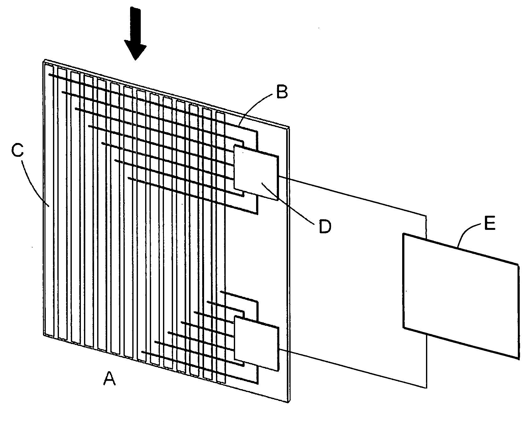
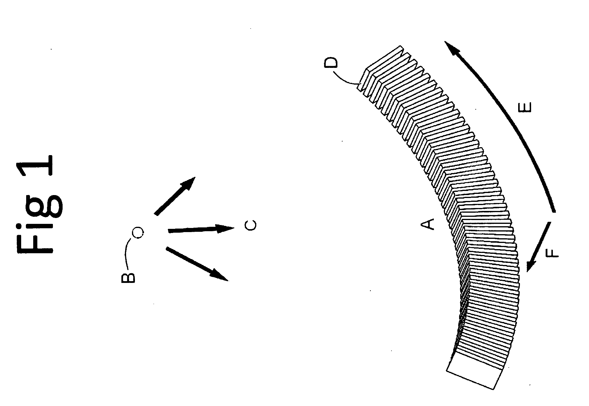
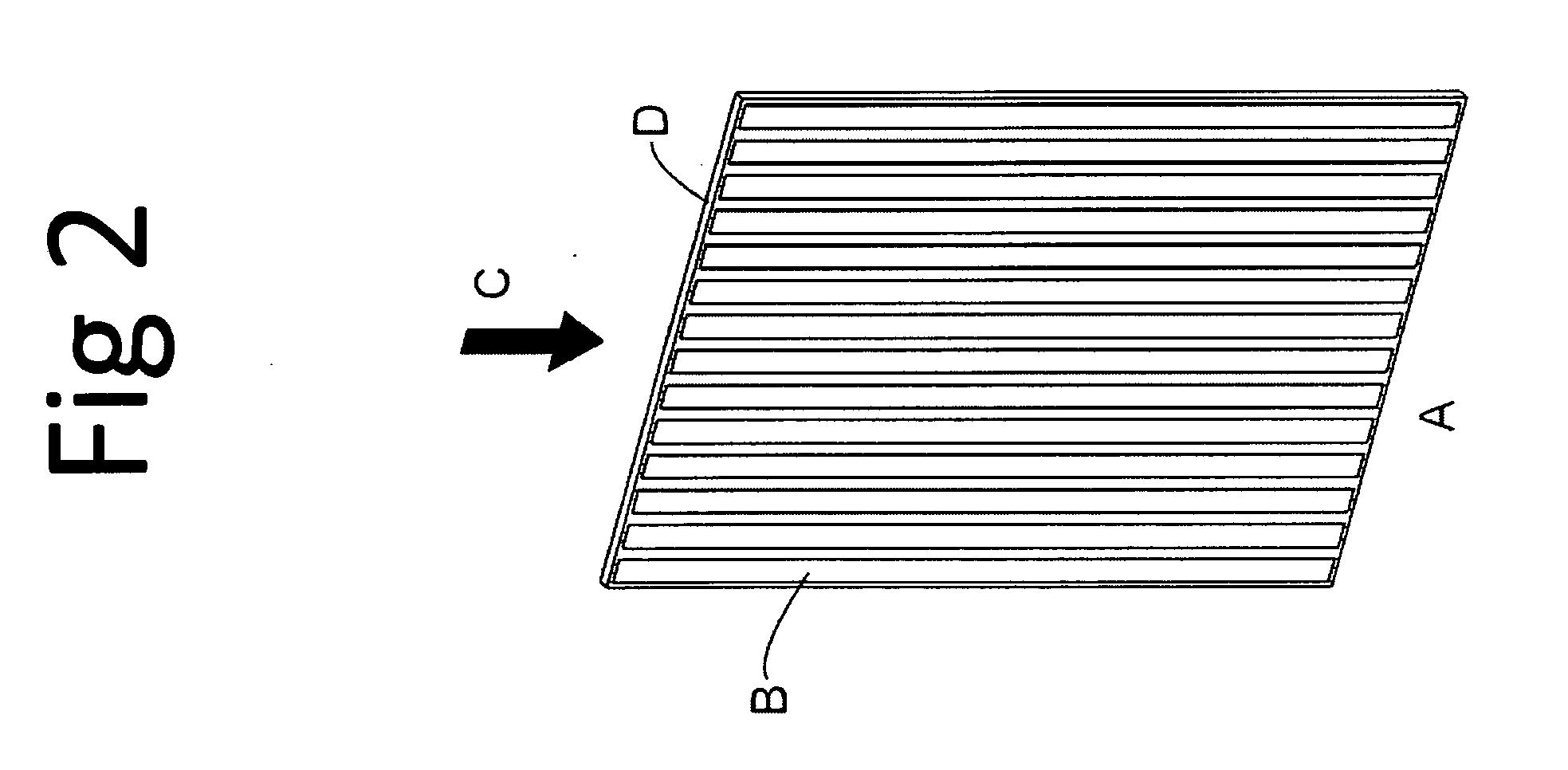
[0042]A basic idea is to provide a Silicon detector for x-ray imaging that is based on multiple semiconductor detector modules arranged together to form an overall detector area, where each semiconductor detector module comprises an x-ray sensor of crystalline Silicon oriented edge-on to incoming x-rays and connected to integrated circuitry for registration of x-rays interacting in the x-ray sensor through the photoelectric effect and through Compton scattering and for an incident x-ray energy between 40 keV and 250 keV to provide the spatial and energy information from these interactions to enable an image of an object. Further, anti-scatter modules are interfolded between at least a subset of the semiconductor detector modules to at least partly absorb Compton scattered x-rays.
[0043]As mentioned, semiconductor detector modules, each including an x-ray sensor, are tiled together to form a full detector of almost arbitrary size with almost perfect geometrical efficiency except for a...
PUM
 Abstract
Description
Claims
Application Information
 - R&D
- Intellectual Property
- Life Sciences
- Materials
- Tech Scout
- Unparalleled Data Quality
- Higher Quality Content
- 60% Fewer Hallucinations
Browse by: Latest US Patents, China's latest patents, Technical Efficacy Thesaurus, Application Domain, Technology Topic, Popular Technical Reports.
© 2025 PatSnap. All rights reserved.Legal|Privacy policy|Modern Slavery Act Transparency Statement|Sitemap|About US| Contact US: help@patsnap.com