Semiconductor power devices manufactured with self-aligned processes and more reliable electrical contacts
- Summary
- Abstract
- Description
- Claims
- Application Information
AI Technical Summary
Benefits of technology
Problems solved by technology
Method used
Image

Examples
Embodiment Construction
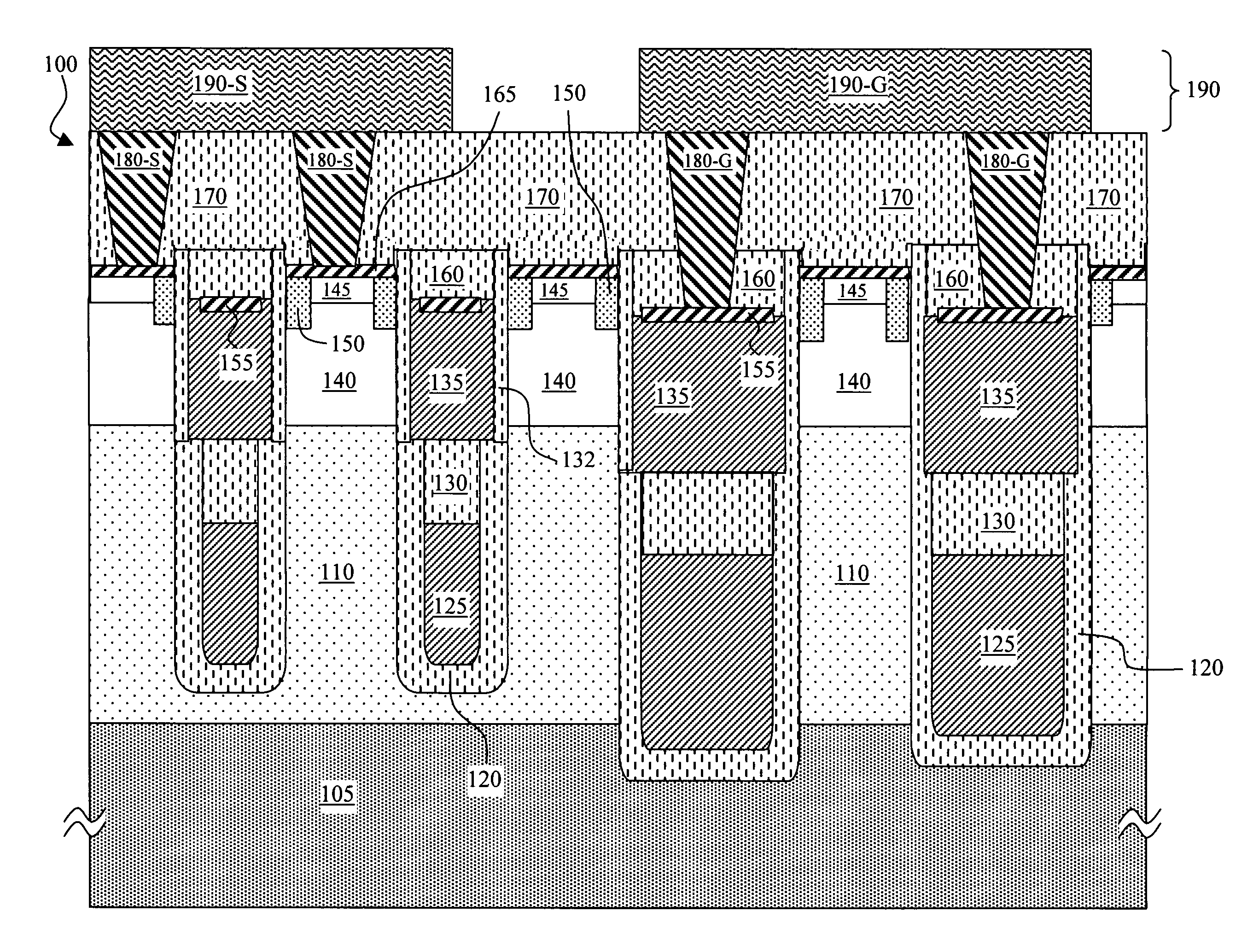
[0032]FIG. 2A shows a cross sectional view of a semiconductor power device, e.g., a trench metal oxide semiconductor field effect transistor (MOSFET) device 100 of this invention. The MOSFET cells are formed in an N-type epitaxial layer 110 supported on an N+ substrate 105. The MOSFET device 100 includes a plurality of trench gates each comprising a bottom polysilicon (poly) segment as a first polysilicon layer 125 padded by a gate insulation layer, e.g., a bottom oxide layer 120 disposed on the bottom portion of the trench. The first polysilicon layer 125 is covered and insulated by an inter-poly dielectric (IPD) layer 130 from a top electrode, e.g., a second polysilicon layer 135. The trench gates are narrower and shallower in the active cell area, covered under the source metal 190-S and generally located near the center of the substrate. The trenches are wider and deeper in certain areas, e.g., in a termination area near the peripheral areas of the substrate, to function as gate...
PUM
 Abstract
Description
Claims
Application Information
 - R&D
- Intellectual Property
- Life Sciences
- Materials
- Tech Scout
- Unparalleled Data Quality
- Higher Quality Content
- 60% Fewer Hallucinations
Browse by: Latest US Patents, China's latest patents, Technical Efficacy Thesaurus, Application Domain, Technology Topic, Popular Technical Reports.
© 2025 PatSnap. All rights reserved.Legal|Privacy policy|Modern Slavery Act Transparency Statement|Sitemap|About US| Contact US: help@patsnap.com