Chip package with plank stack of semiconductor dies
a technology of semiconductor dies and chip packages, applied in semiconductor devices, semiconductor/solid-state device details, electrical devices, etc., can solve the problems of difficult to obtain low-cost, high-performance (e.g., high-bandwidth) interconnections between stacked chips, and the cost of tsvs is typically higher than the cost of wire bonds, so as to facilitate electrical coupling
- Summary
- Abstract
- Description
- Claims
- Application Information
AI Technical Summary
Benefits of technology
Problems solved by technology
Method used
Image

Examples
Embodiment Construction
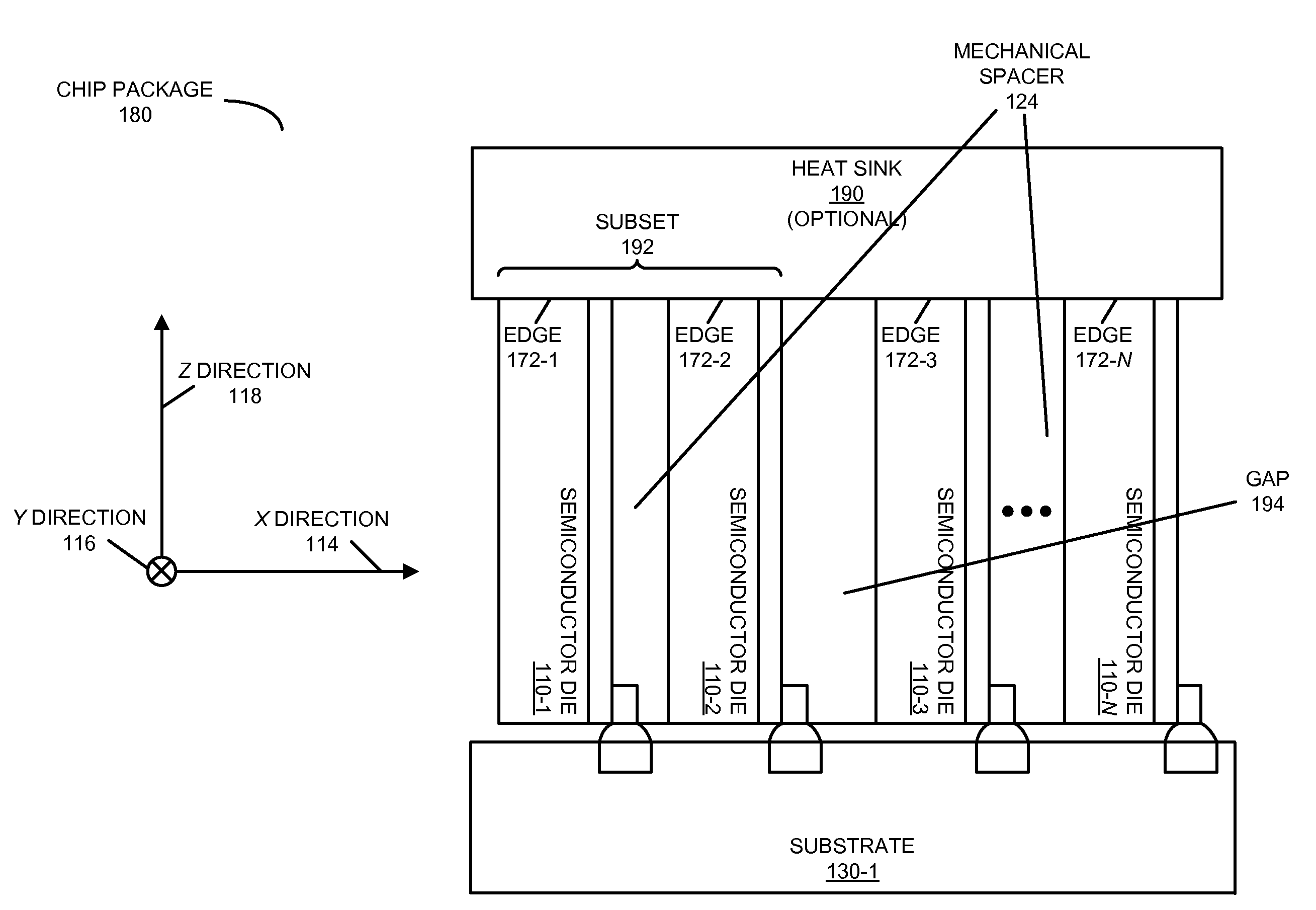
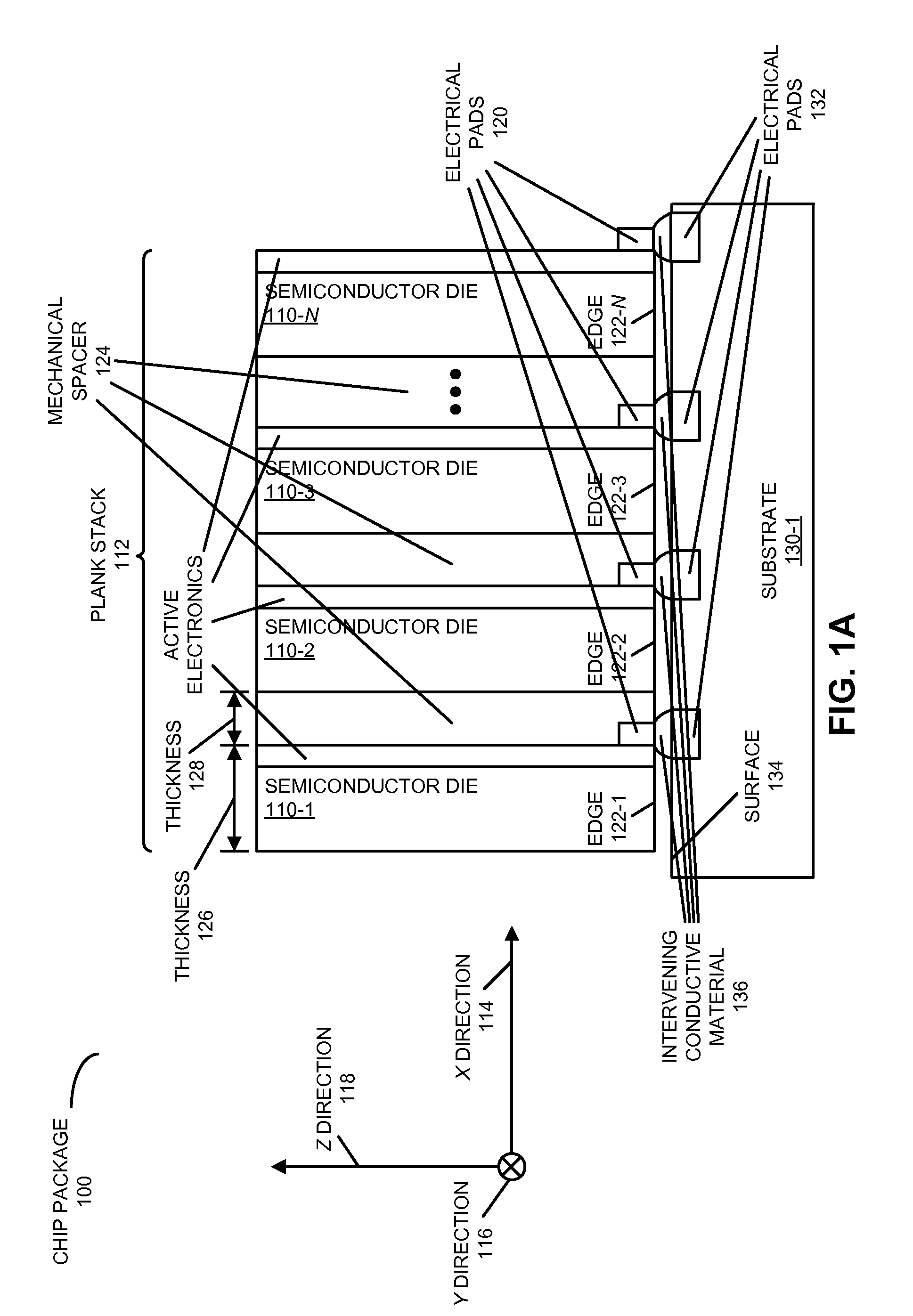
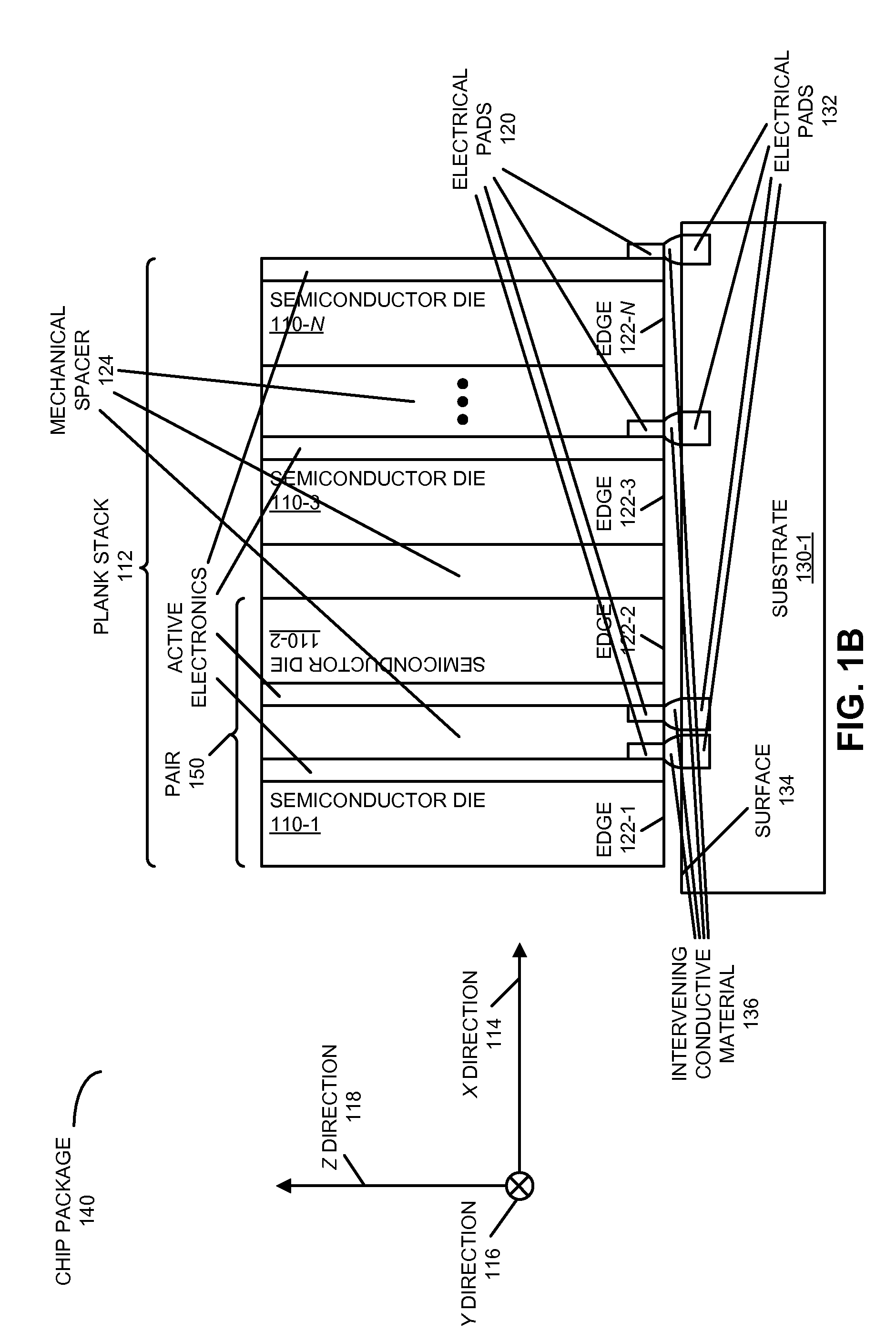
[0050]Embodiments of a chip package, a system that includes the chip package, and a method for fabricating a plank stack of semiconductor dies in the chip package are described. In this chip package, semiconductor dies in a vertical stack of semiconductor dies or chips (which is referred to as a ‘plank stack’) are separated by a mechanical spacer (such as a filler material or an adhesive). Moreover, the chip package includes a substrate at a right angle to the plank stack, which is electrically coupled to the semiconductor dies along an edge of the plank stack. In particular, electrical pads proximate to a surface of the substrate (which are along a stacking direction of the plank stack) are electrically coupled to pads that are proximate to edges of the semiconductor dies by an intervening conductive material, such as: solder, stud bumps, plated traces, wire bonds, spring connectors, traces defined using tape automated bonding, a conductive adhesive and / or an anisotropic conducting...
PUM
 Abstract
Description
Claims
Application Information
 - R&D
- Intellectual Property
- Life Sciences
- Materials
- Tech Scout
- Unparalleled Data Quality
- Higher Quality Content
- 60% Fewer Hallucinations
Browse by: Latest US Patents, China's latest patents, Technical Efficacy Thesaurus, Application Domain, Technology Topic, Popular Technical Reports.
© 2025 PatSnap. All rights reserved.Legal|Privacy policy|Modern Slavery Act Transparency Statement|Sitemap|About US| Contact US: help@patsnap.com