Lateral double-diffused metal-oxide-semiconudctor transistor device and layout pattern for ldmos transistor device
- Summary
- Abstract
- Description
- Claims
- Application Information
AI Technical Summary
Benefits of technology
Problems solved by technology
Method used
Image

Examples
Embodiment Construction
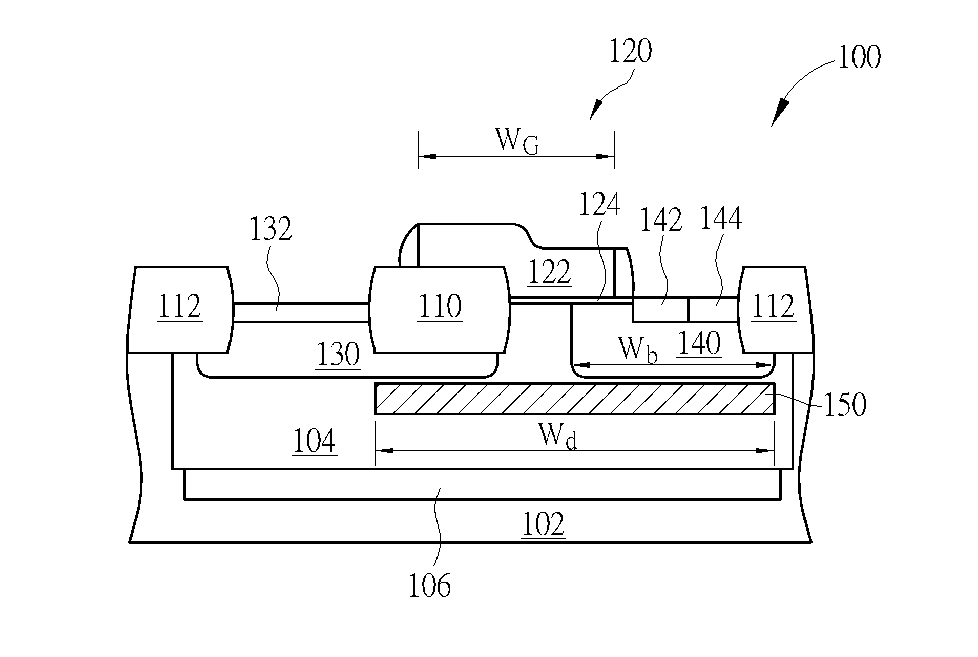
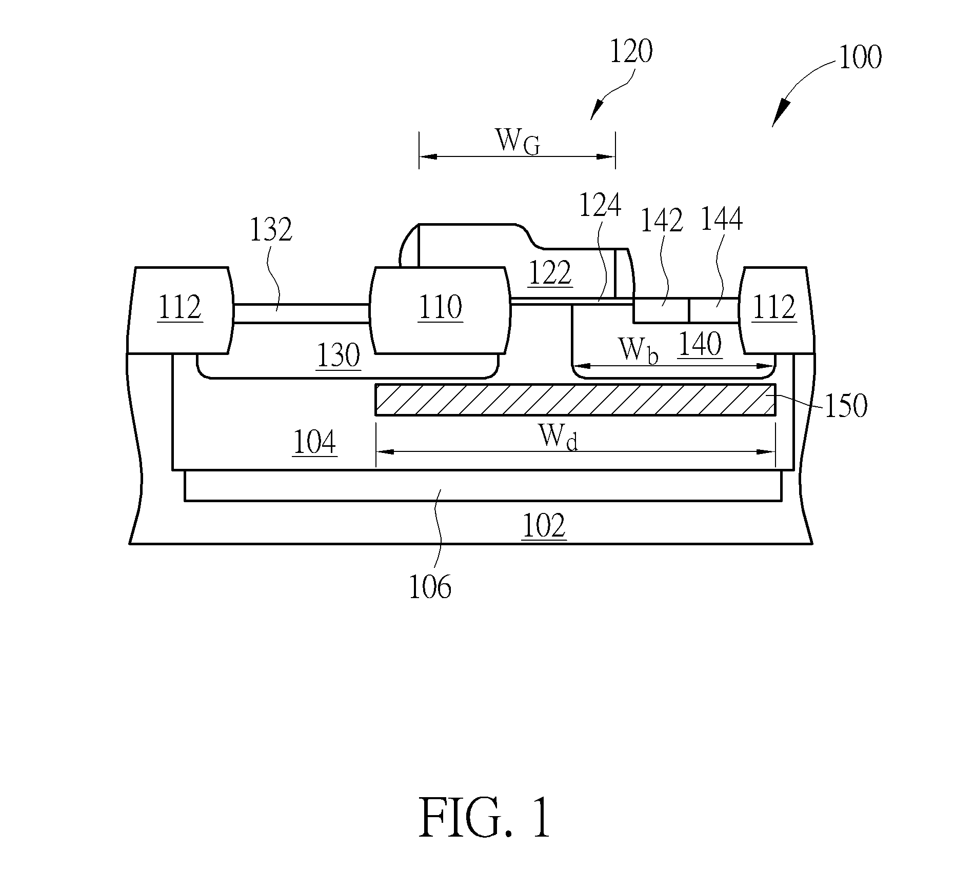
[0015]Please refer to FIG. 1, which is a cross-sectional view of a LDMOS transistor device provided by a first preferred embodiment of the present invention. As shown in FIG. 1, a LDMOS transistor device 100 provided by the first preferred embodiment includes a substrate 102, such as a silicon substrate. A deep well region 104 is formed in the substrate 102 and a buried doped layer 106 is formed under the deep well region 104. The deep well region 104 and the buried doped layer 106 include a first conductivity type, and the substrate 102 includes a second conductivity type. The first conductivity type and the second conductivity type are complementary to each other. In the preferred embodiment, the first conductivity type is an n type and the second conductivity type is a p-type.
[0016]Please still refer to FIG. 1. The LDMOS transistor device 100 further includes a first insulating structure 110 formed in the substrate 102, and a gate 120 positioned on the substrate 102 and covering ...
PUM
 Abstract
Description
Claims
Application Information
 - R&D
- Intellectual Property
- Life Sciences
- Materials
- Tech Scout
- Unparalleled Data Quality
- Higher Quality Content
- 60% Fewer Hallucinations
Browse by: Latest US Patents, China's latest patents, Technical Efficacy Thesaurus, Application Domain, Technology Topic, Popular Technical Reports.
© 2025 PatSnap. All rights reserved.Legal|Privacy policy|Modern Slavery Act Transparency Statement|Sitemap|About US| Contact US: help@patsnap.com