Method for preparing seed crystal including protective film, method for producing ingot using seed crystal, seed crystal including protective film, and method for attaching seed crystal
a technology of protective film and seed crystal, which is applied in the direction of single crystal growth, after-treatment, chemistry apparatus and processes, etc., can solve the problems of difficult to produce high-quality silicon carbide single crystal, hidden defects such as macroscopic channels or voids,
- Summary
- Abstract
- Description
- Claims
- Application Information
AI Technical Summary
Benefits of technology
Problems solved by technology
Method used
Image


Examples
production example 1
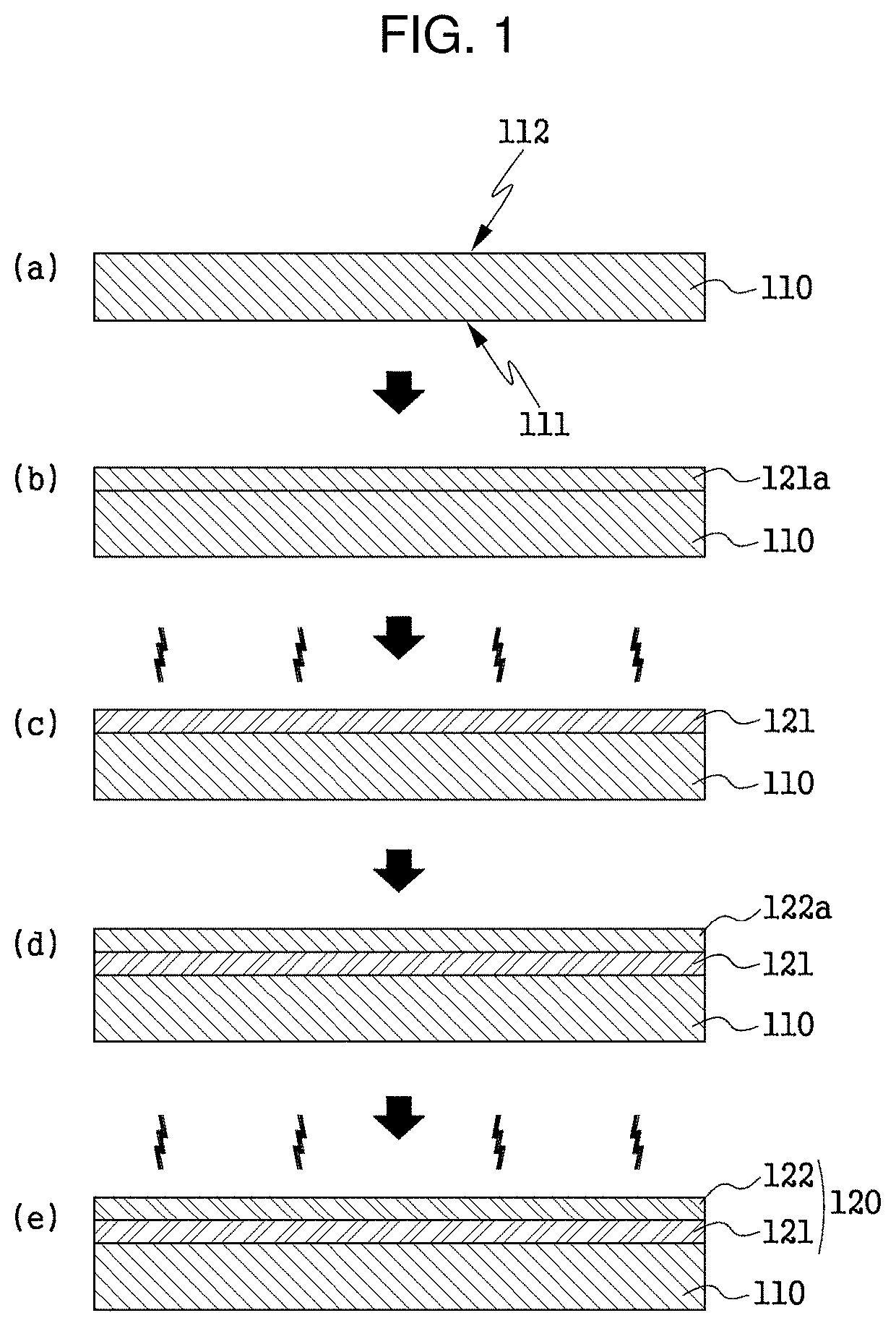
Example 1: Preparation of Seed Crystal Including Protective Film According to Example Embodiments
[0242]1) Preparation of First Layer Composition and Second Layer Composition
[0243]A phenolic resin (KC-5536, Kangnam Chemical Co. Ltd., hereinafter the same applied) as a binder resin was diluted with ethanol (OCI, hereinafter the same applied) as a solvent to prepare a first layer composition having a solid content of ˜10 wt %.
[0244]The binder resin was diluted with the solvent until a solid content of ˜10 wt % was reached. Thereafter, the dilution was mixed with a filler (crystalline graphite, purity 80-99%, D50 2.5 μm, hereinafter the same applied). The filler was used in an amount of ˜90 parts by weight, based on 100 parts by weight of the binder resin. The resulting mixture was mixed with 5 parts by weight of additives, including a wetting dispersant and a defoamer, and dispersed to obtain a second layer composition.
[0245]2) Formation of First Layer
[0246]The first layer composition ...
production example 2
Example 1
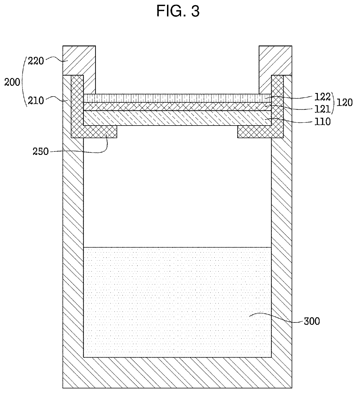
[0266]Components used in Example 1 and Comparative Example 1 of Production Example 2 are as follows:[0267]Liquid phenolic resin: phenolic resin / methyl alcohol / water=58-62:36-41:0-4 (weight ratio), Neolite KC-4703, Kangnam Chemical Co. Ltd.[0268]Crystalline graphite: Average particle size (D50)=2.5 μm[0269]Silicon carbide seed crystal: Diameter=4-6 inches, thickness=500-1200 μm, crystal structure=4H single crystal substrate[0270]Seed crystal holder: Diameter=7 inches, thickness=5-10 mm
[0271]Preparation of Seed Crystal with Protective Layer and Adhesive Layer
[0272]The liquid phenolic resin was mixed with the crystalline graphite as a filler in a weight ratio of 7:3 and 100 parts by weight of the mixture was mixed with 3 parts by weight of additives, including a wetting dispersant and a defoamer. The resulting mixture was dispersed to obtain a protective layer composition. The protective layer composition was spin coated on one surface of the silicon carbide seed crystal to fo...
PUM
 Abstract
Description
Claims
Application Information
 - R&D
- Intellectual Property
- Life Sciences
- Materials
- Tech Scout
- Unparalleled Data Quality
- Higher Quality Content
- 60% Fewer Hallucinations
Browse by: Latest US Patents, China's latest patents, Technical Efficacy Thesaurus, Application Domain, Technology Topic, Popular Technical Reports.
© 2025 PatSnap. All rights reserved.Legal|Privacy policy|Modern Slavery Act Transparency Statement|Sitemap|About US| Contact US: help@patsnap.com