Method of manufacturing semiconductor package including forming a resin sealing member
- Summary
- Abstract
- Description
- Claims
- Application Information
AI Technical Summary
Benefits of technology
Problems solved by technology
Method used
Image

Examples
Embodiment Construction
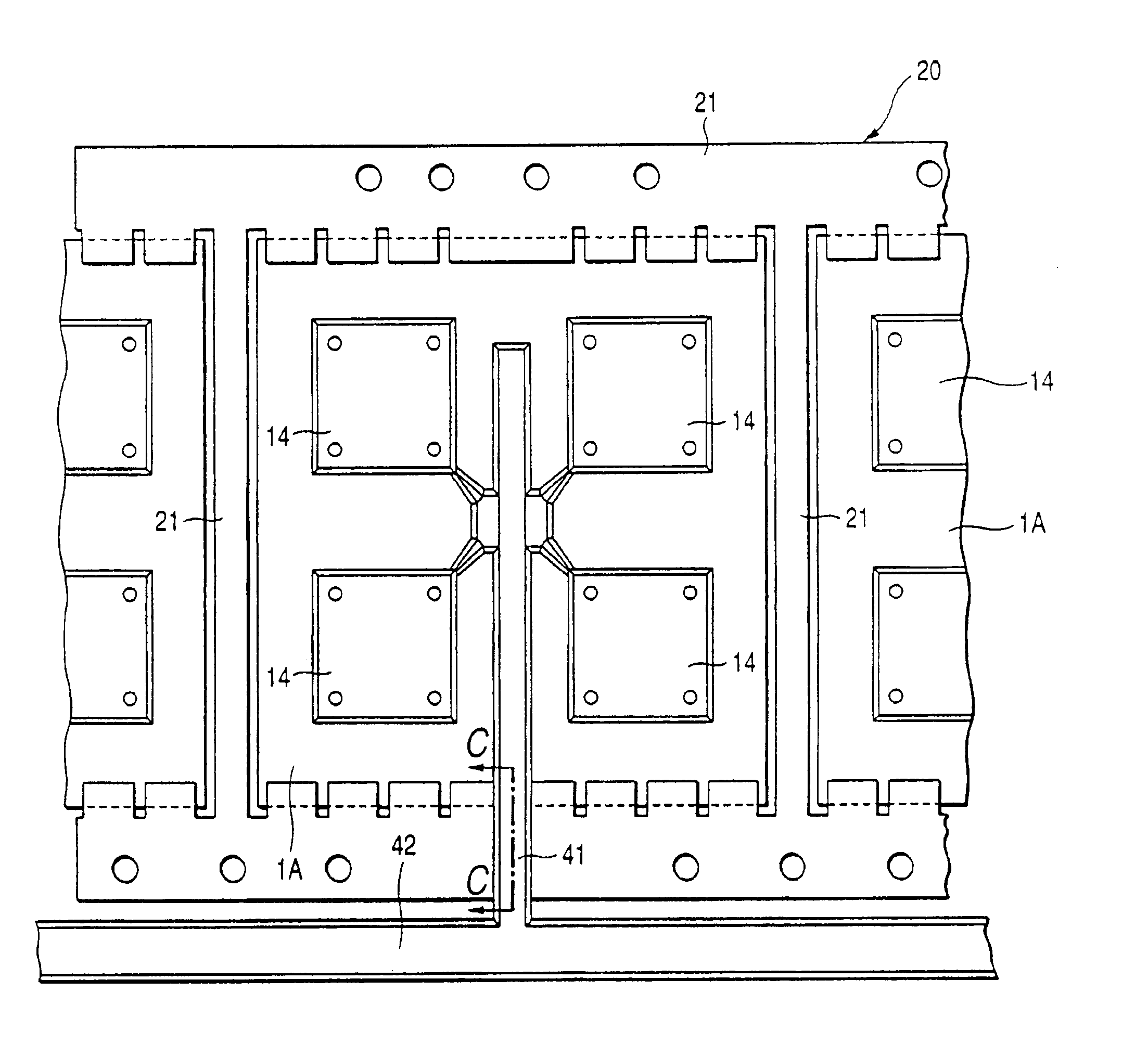
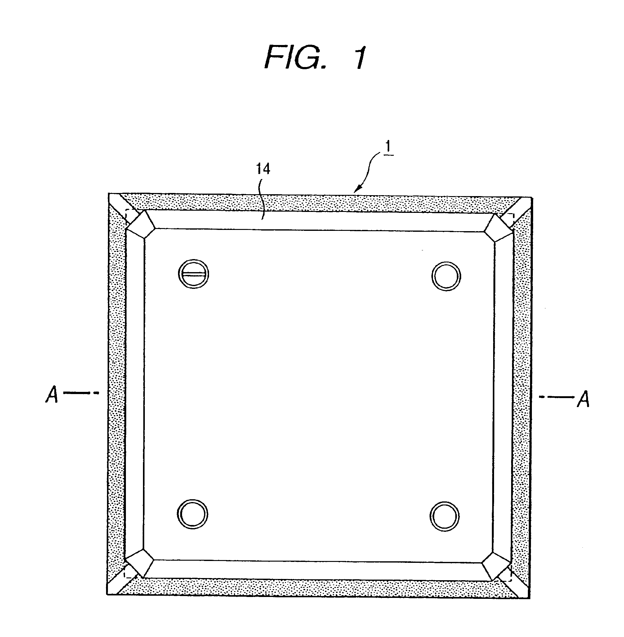
[0053]An embodiment of this invention, which is applicable to a semiconductor device having a BGA structure, will be explained. The same reference numerals are used to identify elements having the same function in the several drawings and repeated explanation of such elements is omitted in this description.
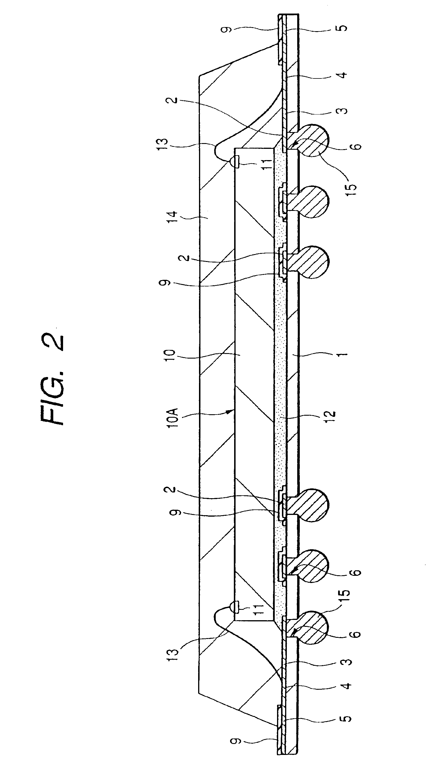
[0054]FIG. 1 is a plan view of a semiconductor device representing one embodiment of this invention. FIG. 2 shows an enlarged sectional view taken along the A—A line in FIG. 1. FIG. 3 is an enlarged sectional view of part of FIG. 2. FIG. 4 is a plan view which shows the device with the resin sealing body removed. FIG. 5 is a plan view of the base substrate. FIG. 6 is an enlarged sectional view of part of the semiconductor device.
[0055]As shown in FIG. 1, FIG. 2 and FIG. 3, the semiconductor device has the following structure. Semiconductor chip 10 is mounted by using adhesive material 12 on the chip mount area of the main surface of a base substrate 1. And, several bump electrodes...
PUM
 Abstract
Description
Claims
Application Information
 - R&D
- Intellectual Property
- Life Sciences
- Materials
- Tech Scout
- Unparalleled Data Quality
- Higher Quality Content
- 60% Fewer Hallucinations
Browse by: Latest US Patents, China's latest patents, Technical Efficacy Thesaurus, Application Domain, Technology Topic, Popular Technical Reports.
© 2025 PatSnap. All rights reserved.Legal|Privacy policy|Modern Slavery Act Transparency Statement|Sitemap|About US| Contact US: help@patsnap.com