Semiconductor high-voltage devices
a high-voltage device and semiconductor technology, applied in the direction of semiconductor devices, electrical equipment, transistors, etc., can solve the problem of no significant improvemen
- Summary
- Abstract
- Description
- Claims
- Application Information
AI Technical Summary
Benefits of technology
Problems solved by technology
Method used
Image

Examples
Embodiment Construction
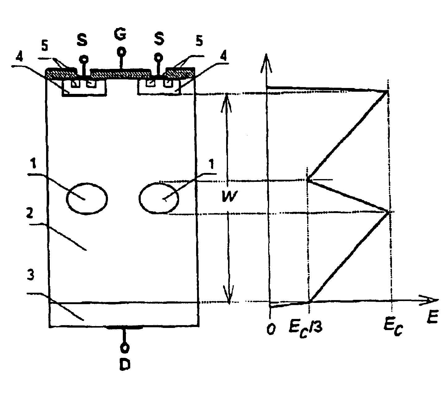
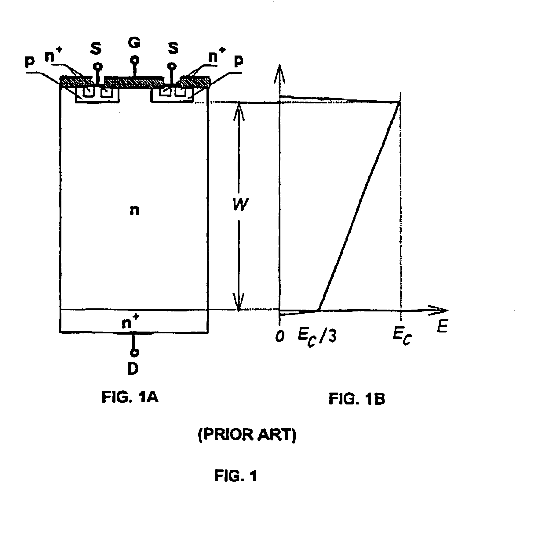
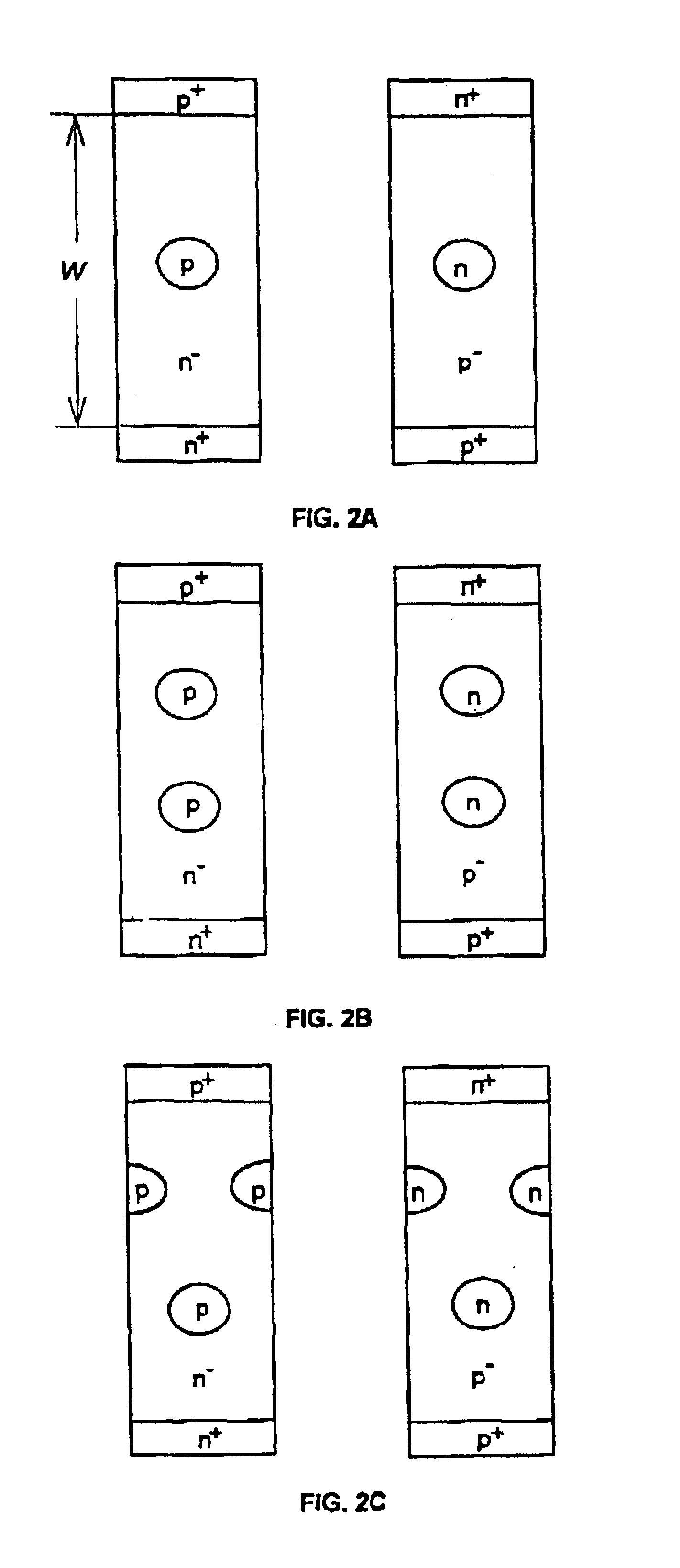
[0023]FIG. 2 shows several structures of a voltage sustaining layer according to the invention.
[0024]In FIG. 2A, a voltage sustaining layer with p (or n) islands in a plane is shown (i.e., n=2, two sub-layers). In FIG. 2B, a voltage sustaining layer with p (or n) islands disposed in two planes is shown (i.e., n=3, three sub-layers), where each island in the upper plane is vertically arranged over a corresponding island in the lower plane. FIG. 2C shows another voltage sustaining layer with two planes of p (or n) islands (n=3), wherein each of islands in the upper plane is vertically arranged in the middle of two neighboring islands in the lower plane.
[0025]The horizontal layout of the voltage sustaining layer than be either interdigitated (finger), or hexagonal (cell), or rectangular (cell). In all the figures of schematic cross-sectional view of the structures, only one or two units (fingers or cells) of the voltage sustaining layer are shown.
[0026]The voltage sustaining layer of t...
PUM
 Abstract
Description
Claims
Application Information
 - R&D
- Intellectual Property
- Life Sciences
- Materials
- Tech Scout
- Unparalleled Data Quality
- Higher Quality Content
- 60% Fewer Hallucinations
Browse by: Latest US Patents, China's latest patents, Technical Efficacy Thesaurus, Application Domain, Technology Topic, Popular Technical Reports.
© 2025 PatSnap. All rights reserved.Legal|Privacy policy|Modern Slavery Act Transparency Statement|Sitemap|About US| Contact US: help@patsnap.com