Such packages are often very small as compared to more conventional
integrated circuit device packages (e.g., BGAs, PLCC, QFP, PGA) for conventional large DSPs (
digital signal processors), ASICs (
application specific integrated circuits), memory devices (e.g., Flash,
DRAM, ROM) for computers, microprocessors (e.g., Intel™
Pentium), and the like, which often use very high pin counts and extremely large die sizes.
Although there has been much development with package designs for conventional devices, to date there has been little focus on improving the design of packages for the smaller,
low pin count and low integration devices, especially for power applications.
Many conventional
small footprint packages still lack efficiency and performance.
For example, conventional packages have not been configured to provide enhanced performance per unit area of PC board occupied.
This poor area efficiency limits the functionality or performance of the
semiconductor component in its application, especially when the available board space is determined by the maximum allowable size and three-dimensional form-factor of the end product, such as a
cell phone.
In this context, poor performance may constitute a lack of desirable features in the
semiconductor (features not possible because of a limited amount of available
silicon real estate), or as a higher resistance device,
transistor,
power MOSFET or other switching element leading to increased power losses,
self heating, and further increases in resistance as a result of
self heating.
These increased power losses can be viewed as both a potential
thermal problem, and as a loss in efficiency and battery life.
Furthermore, such small, low-pin count packages typically lack sufficient ability to remove heat from the
semiconductor die and to conduct that heat out of the package into the PC board and into the ambient.
The high
thermal resistance characteristic of a package's inability to remove heat limits the utility of these conventional type small packages in applications (and in products) where the semiconductor die is forced to dissipate substantial power, even if but for a few seconds.
In high power dissipation conditions, unless the power dissipation is limited, the semiconductor die may malfunction, or be damaged, and may also damage its own package and even other components in its vicinity on the PC board.
As a further limitation of such conventional packages, methods used to increase the number of potential pins on any given package, may in fact reduce the maximum die size that can fit into the package, and in so doing lead to even
higher power losses and lower efficiencies.
It can also be shown, that adjusting the
lead frame design in a conventional package to maximize the die size, may in fact lead to an inadequate number of pins to connect the IC or die, and may also result in the position of such pins and bond pads such that it becomes difficult or impossible to facilitate proper or optimal
wire bonding.
Likewise, it can be shown that adjusting the number of pins for optimum bonding may result in a smaller die and poorer
silicon performance, for example increasing the resistance in a power
transistor, and in other cases, may result in a higher
thermal resistance in a package with no convenient means to conduct heat out of the
silicon and into the
printed circuit board (PCB).
Any or all of these factors make it difficult to achieve optimal performance for many IC and discrete devices, especially those involved in power applications or carrying
high current.
The conventional package occupies less than 10% of the entire package
footprint on the PC board, which is undesirable for today's high performance applications.
The conventional package is also not configured in a manner to efficiently draw away
thermal energy that may dissipate or build up in certain types of
power integrated circuits and in discrete power devices.
Accordingly, conventional six lead packages have many limitations.
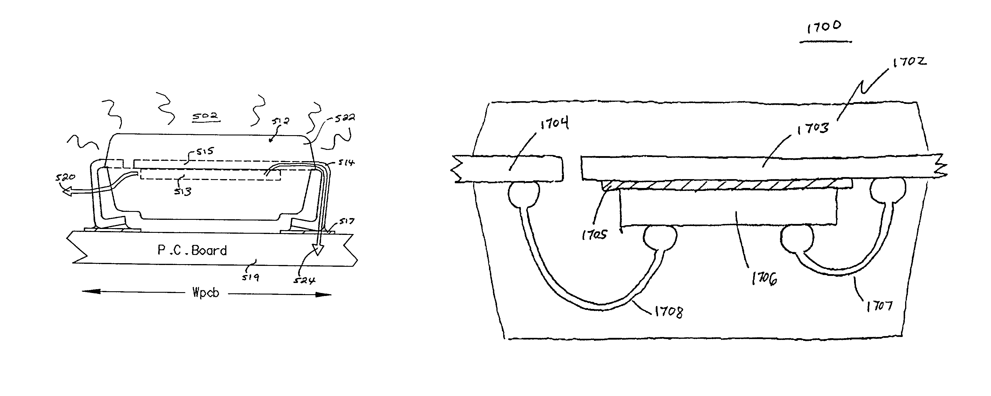
Accordingly a
single lead, such as 128, connected directly to the die pad, while improving thermal resistance, results in less improvement than expected and depends heavily on the PC board
layout.
Although a larger pin (or multiple pins) carrying heat would be less sensitive to the influence of the board
layout on the resulting thermal resistance, such design features are not available or anticipated by conventional packages.
Another drawback with this configuration of a six-lead package is it still lacks an ability to efficiently use package space.
