Semiconductor device
a semiconductor and device technology, applied in the field of semiconductor devices, can solve problems such as cross-sectional area, and achieve the effect of reducing the overall size of a semiconductor devi
- Summary
- Abstract
- Description
- Claims
- Application Information
AI Technical Summary
Benefits of technology
Problems solved by technology
Method used
Image

Examples
Embodiment Construction
[0033]Preferred embodiments of the present invention will hereinafter be described with reference to the accompanying drawings.
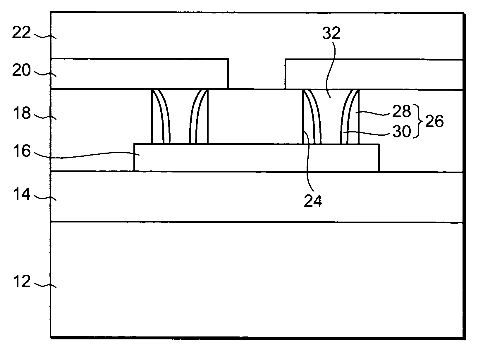
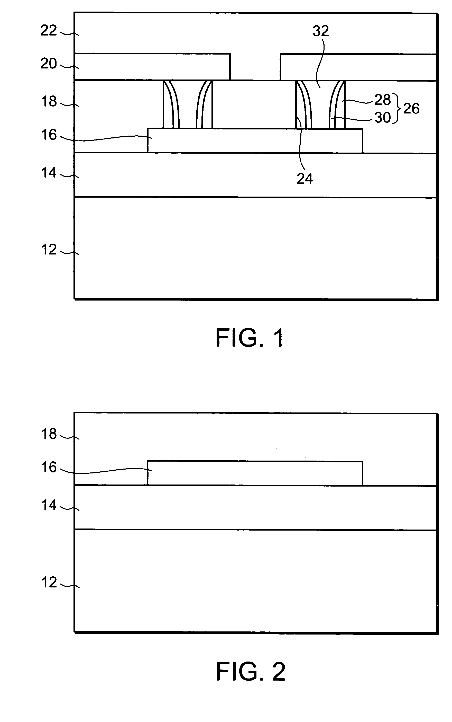
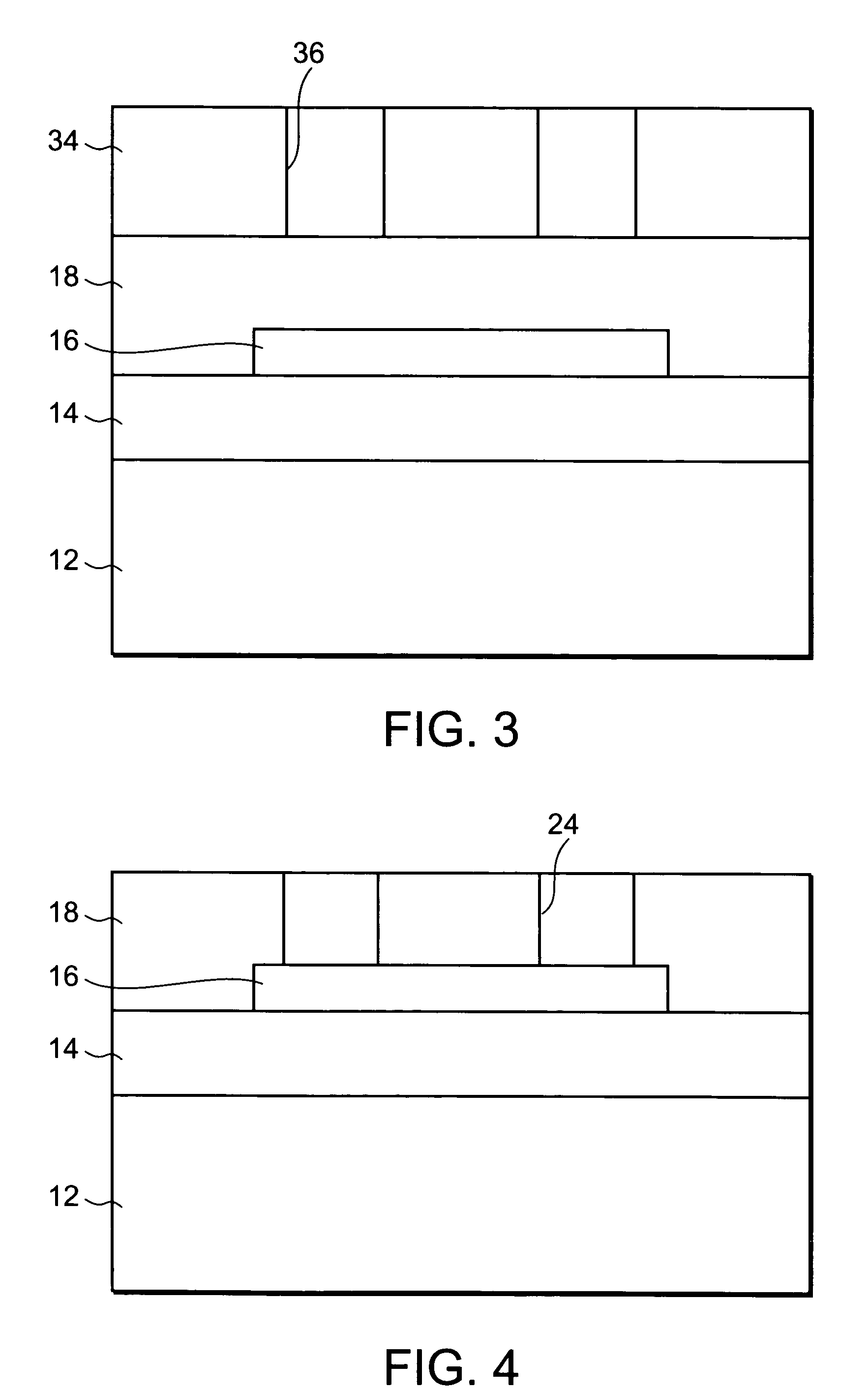
[0034]FIG. 1 shows a semiconductor device 10 according to one embodiment of the present invention. The semiconductor device 10 includes a semiconductor substrate 12, a first insulator layer 14 formed on the semiconductor substrate 12, a first conductive layer 16 formed on the first insulator layer 14, a second insulator layer 18 formed on the first conductive layer 16, a second conductive layer 20 formed on the second insulator layer 18 and a third insulator layer 22 formed on the second conductive layer 20.
[0035]The semiconductor substrate 12 is a silicon substrate. The first insulator layer 14 is formed of silicon oxide.
[0036]The first conductive layer 16 is formed of a metal such as aluminum. The first conductive layer 16 serves as interconnections. The second insulator layer 18 is formed of silicon oxide.
[0037]The second conductive layer 20 is formed of ...
PUM
 Abstract
Description
Claims
Application Information
 - R&D
- Intellectual Property
- Life Sciences
- Materials
- Tech Scout
- Unparalleled Data Quality
- Higher Quality Content
- 60% Fewer Hallucinations
Browse by: Latest US Patents, China's latest patents, Technical Efficacy Thesaurus, Application Domain, Technology Topic, Popular Technical Reports.
© 2025 PatSnap. All rights reserved.Legal|Privacy policy|Modern Slavery Act Transparency Statement|Sitemap|About US| Contact US: help@patsnap.com