Magnetoresistive element and magnetic memory
a magnetic memory and magnetoresistive element technology, applied in the field of magnetoresistive element and magnetic memory, can solve problems such as difficulty in providing a sufficient magnetic field
- Summary
- Abstract
- Description
- Claims
- Application Information
AI Technical Summary
Benefits of technology
Problems solved by technology
Method used
Image

Examples
first embodiment
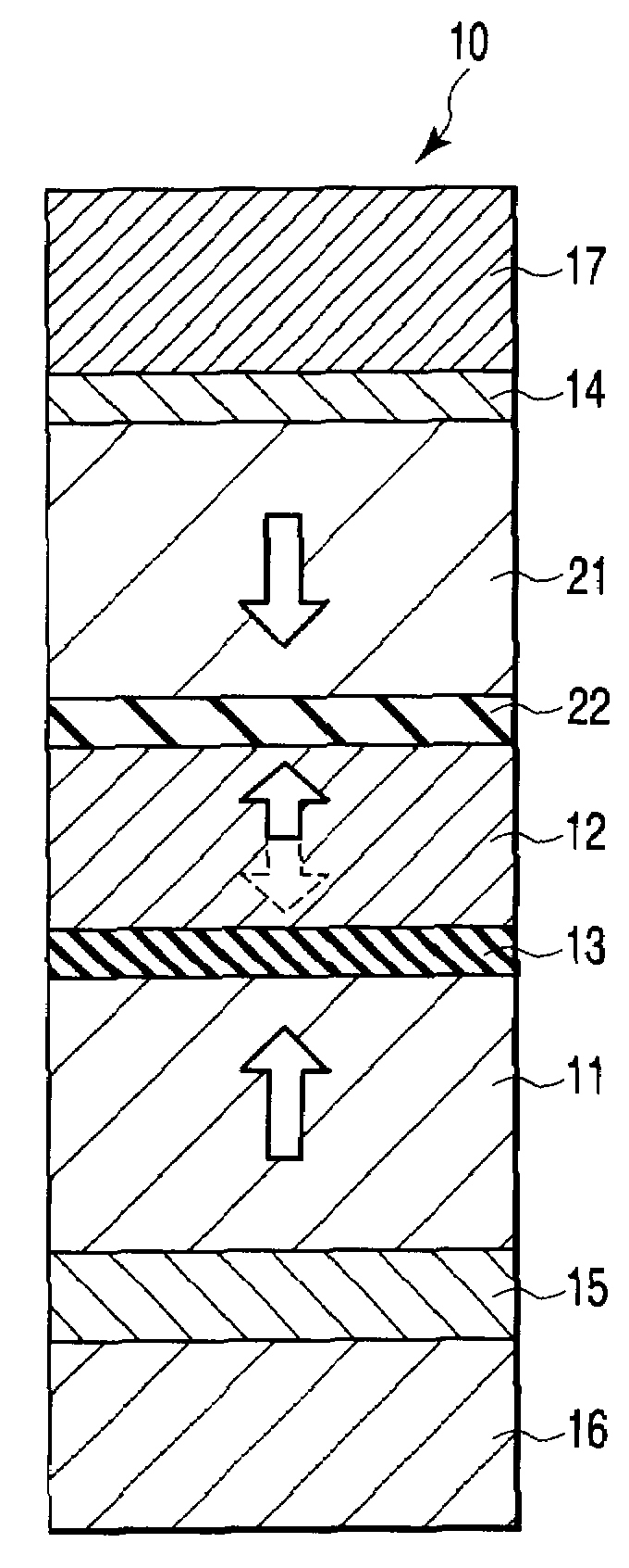
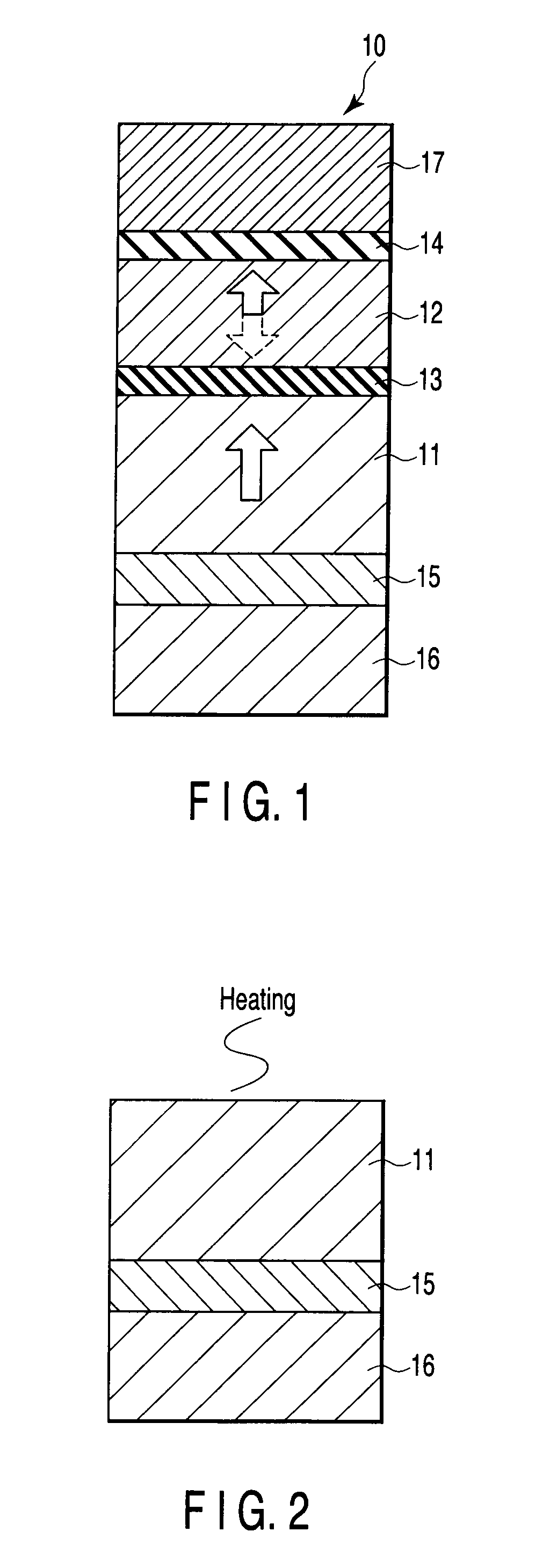
[0060]FIG. 1 is a sectional view illustrating the structure of an MTJ element 10 according to the first embodiment. Arrows in FIG. 1 indicate magnetization directions. In this embodiment, the MTJ element 10 having a single pinned layer structure (i.e., a structure that arranges a free layer and a pinned layer on both sides of a nonmagnetic layer) will be described.
[0061]The MTJ element 10 has a layered structure formed by sequentially stacking a crystal orientation underlayer 15, fixed layer (also referred to as a magnetization fixed layer or pinned layer) 11, tunnel barrier layer (nonmagnetic layer) 13, recording layer (also referred to as a magnetization free layer or free layer) 12, and cap layer 14. The layered structure may have a reversed stacking order. A lower electrode 16 is provided on the lower surface of the crystal orientation underlayer 15. An upper electrode 17 is provided on the upper surface of the cap layer 14.
[0062]The fixed layer 11 has a fixed magnetization (or ...
second embodiment
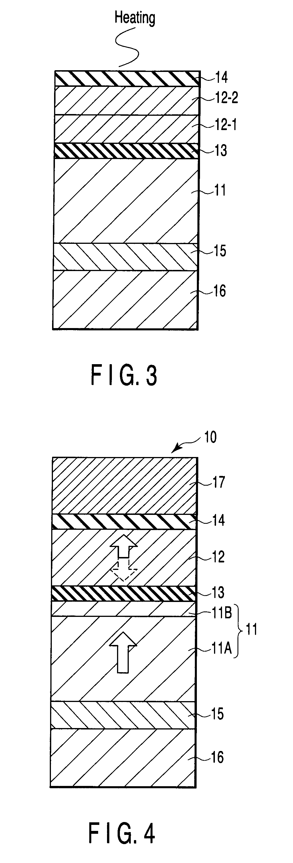
[0117]In the second embodiment, a magnetic layer to control the crystallinity of a tunnel barrier layer 13 is inserted between the tunnel barrier layer 13 and a fixed layer 11, thereby improving the crystallinity of the tunnel barrier layer 13 and a recording layer 12.
[0118]FIG. 4 is a sectional view illustrating the structure of an MTJ element 10 according to the second embodiment. In this embodiment, the MTJ element 10 having a single pinned layer structure will be described.
[0119]The MTJ element 10 has a layered structure formed by sequentially stacking a crystal orientation underlayer 15, fixed layer 11A, interface fixed layer 11B, tunnel barrier layer 13, recording layer 12, and cap layer 14. The layered structure may have a reversed stacking order. A lower electrode 16 is provided on the lower surface of the crystal orientation underlayer 15. An upper electrode 17 is provided on the upper surface of the cap layer 14.
[0120]The fixed layer 11 of this embodiment is formed by stac...
third embodiment
[0122]In the third embodiment, a magnetic layer to enhance the magnetoresistive effect is inserted between a recording layer 12 and a tunnel barrier layer 13, thereby improving the characteristic of an MTJ element 10.
[0123]FIG. 5 is a sectional view illustrating the structure of the MTJ element 10 according to the third embodiment. In this embodiment, the MTJ element 10 having a single pinned layer structure will be described.
[0124]The MTJ element 10 has a layered structure formed by sequentially stacking a crystal orientation underlayer 15, fixed layer 11, tunnel barrier layer 13, interface recording layer 12B, recording layer 12A, and cap layer 14. The layered structure may have a reversed stacking order. A lower electrode 16 is provided on the lower surface of the crystal orientation underlayer 15. An upper electrode 17 is provided on the upper surface of the cap layer 14.
[0125]The recording layer 12 of this embodiment is formed by stacking the interface recording layer 12B and r...
PUM
 Abstract
Description
Claims
Application Information
 - R&D
- Intellectual Property
- Life Sciences
- Materials
- Tech Scout
- Unparalleled Data Quality
- Higher Quality Content
- 60% Fewer Hallucinations
Browse by: Latest US Patents, China's latest patents, Technical Efficacy Thesaurus, Application Domain, Technology Topic, Popular Technical Reports.
© 2025 PatSnap. All rights reserved.Legal|Privacy policy|Modern Slavery Act Transparency Statement|Sitemap|About US| Contact US: help@patsnap.com