Semiconductor device having semiconductor chips stacked and mounted thereon and manufacturing method thereof
a semiconductor chip and semiconductor technology, applied in semiconductor devices, semiconductor/solid-state device details, electrical devices, etc., can solve the problems of difficult to deal with the wafer, easy to crack or chip cracking, and easy to chip cracking
- Summary
- Abstract
- Description
- Claims
- Application Information
AI Technical Summary
Benefits of technology
Problems solved by technology
Method used
Image

Examples
first embodiment
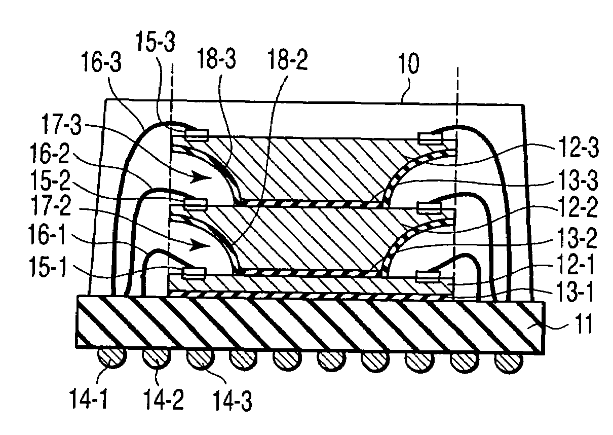
[0168]FIG. 1 is a cross sectional view showing a semiconductor device according to a first embodiment of this invention. In this case, a stack MCP having three semiconductor chips with the same size stacked is dealt with as an example. That is, three semiconductor chips 12-1, 12-2, 12-3 with the same size are stacked and mounted on a printed circuit board (PCB) 11 with DAFs 13-1, 13-2, 13-3 disposed therebetween, respectively. For example, the circuit board 11 has a multi-layered wiring structure. Wirings to which bonding wires are connected are formed on the chip mounting surface of the circuit board 11 and external connection electrodes (external terminals) 14-1, 14-2, 14-3, . . . such as ball bumps (solder balls) and pins are arranged in an array form on the backside thereof to form a so-called ball grid array or pin grid array.
[0169]Bonding pads 15-1, 15-2, 15-3 formed on the main surfaces of the semiconductor chips 12-1, 12-2, 12-3 and the printed wirings formed on the chip mou...
second embodiment
[0355]FIG. 124 is a cross sectional view of a semiconductor device according to a second embodiment of this invention. In this case, a COC package type semiconductor device having three semiconductor chips with the same size stacked is taken as an example. Three semiconductor chips 12-1, 12-2, 12-3 with the same size are stacked and mounted on a circuit board 11 with DAFs (die attach films) 13-1, 13-2, 13-3 disposed therebetween, respectively. For example, the circuit board 11 has a multi-layered wiring structure. Electrode pads on which stud bumps 56-1 are formed are provided on the chip mounting surface of the circuit board 11 and external connection electrodes 14-1, 14-2, 14-3, . . . such as solder balls and pins are arranged in an array form on the backside of the chip to form a so-called ball grid array or pin grid array.
[0356]Through electrodes 55-1, 55-2, 55-3 formed of copper (Cu), gold (Au), tungsten (W) or polysilicon are provided along the two (or four) opposite sides of ...
PUM
 Abstract
Description
Claims
Application Information
 - R&D
- Intellectual Property
- Life Sciences
- Materials
- Tech Scout
- Unparalleled Data Quality
- Higher Quality Content
- 60% Fewer Hallucinations
Browse by: Latest US Patents, China's latest patents, Technical Efficacy Thesaurus, Application Domain, Technology Topic, Popular Technical Reports.
© 2025 PatSnap. All rights reserved.Legal|Privacy policy|Modern Slavery Act Transparency Statement|Sitemap|About US| Contact US: help@patsnap.com