Display device and method of driving the same
a display device and display method technology, applied in static indicating devices, cathode-ray tube indicators, instruments, etc., can solve problems such as complex integration circuits, and achieve the effect of reducing the load of an integrated circui
- Summary
- Abstract
- Description
- Claims
- Application Information
AI Technical Summary
Benefits of technology
Problems solved by technology
Method used
Image

Examples
embodiment mode 1
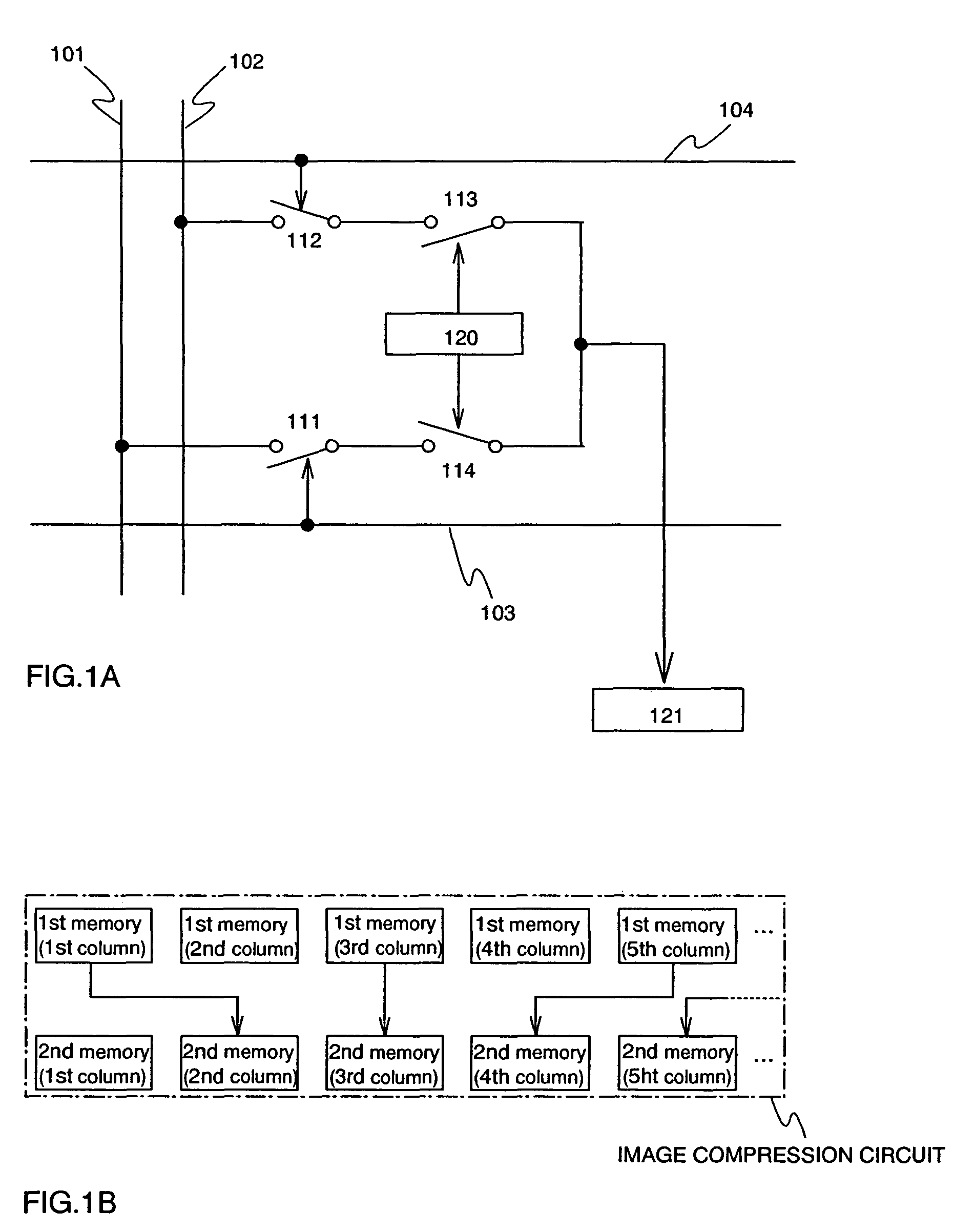
[0039]In this Embodiment Mode, a structure of a pixel portion and a screen compression circuit are described referring to FIG. 1A.
[0040]FIG. 1A shows a pixel structure, which includes: a first signal line (a signal line for a first screen) 101; a first scanning line (a scanning line for the first screen) 103; a first switch 111 in which on / off is controlled based on the information of the first signal line 101 and the first scanning line 103; a second signal line (a signal line for a second screen) 102 and a second scanning line (a scanning line for the second screen) 104; a second switch 112 in which on / off is controlled based on the information of the second signal line 102 and the second scanning line 104; a third switch 113 and a fourth switch 114 in which on / off are controlled based on the information of a memory 120 that are connected to the first switch 111 and the second switch 112 respectively; and a display element 121 connected to the third switch 113 and the fourth switc...
embodiment mode 2
[0054]In this Embodiment Mode, a pixel structure of a multi-window display device having three screens is described referring to FIG. 13.
[0055]FIG. 13 shows a pixel structure, which includes: a first signal line (a signal line for a first screen) 1301; a first scanning line (a scanning line for the first screen) 1304; a first switch 1311 in which on / off is controlled based on the information of the first signal line 1301 and the first scanning line 1304; a second signal line (a signal line for a second screen) 1302 and a second scanning line (a scanning line for the second screen) 1305; a second switch 1312 in which on / off is controlled based on the information of a second signal line 1302 and a second scanning line 1305; a third signal line (a signal line for a third screen) 1303; a third scanning line (a scanning line for the third screen)1306; a third switch 1313 in which on / off is controlled based on the information of the first signal line 1303 and the first scanning line 1306;...
embodiment mode 3
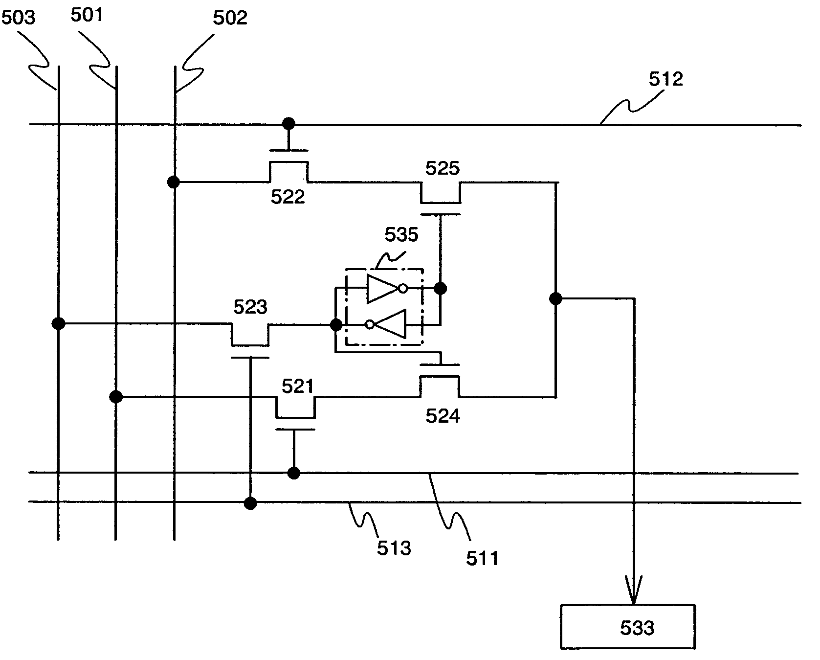
[0058]In this embodiment mode, description will be made of a pixel structure including a signal line and a scanning line for a memory in the case of using a light emitting element with reference to FIGS. 3A and 3B.
[0059]FIG. 3A shows a pixel that includes: a first signal line 301 and a first scanning line 311 for a first screen; a second signal line 302 and a second scanning line 312 for a second screen; a first memory 331 that selects the first scanning line or the second scanning line; a third signal line 303 and a third scanning line 313 for a first memory; a first transistor 321 connected with the first signal line and the first scanning line; a second transistor 322 connected with the second signal line and the second scanning line; a third transistor 323 connected with the third signal line and the third scanning line; a fourth transistor 324 and a fifth transistor 325 which are connected with the first memory and respectively connected with the first transistor and the second...
PUM
 Abstract
Description
Claims
Application Information
 - R&D
- Intellectual Property
- Life Sciences
- Materials
- Tech Scout
- Unparalleled Data Quality
- Higher Quality Content
- 60% Fewer Hallucinations
Browse by: Latest US Patents, China's latest patents, Technical Efficacy Thesaurus, Application Domain, Technology Topic, Popular Technical Reports.
© 2025 PatSnap. All rights reserved.Legal|Privacy policy|Modern Slavery Act Transparency Statement|Sitemap|About US| Contact US: help@patsnap.com