Field programmable gate array architecture having Clos network-based input interconnect
- Summary
- Abstract
- Description
- Claims
- Application Information
AI Technical Summary
Problems solved by technology
Method used
Image

Examples
Embodiment Construction
[0051]Persons of ordinary skill in the art will realize that the following description of the present invention is illustrative only and not in any way limiting. Other embodiments of the invention will readily suggest themselves to such skilled persons.
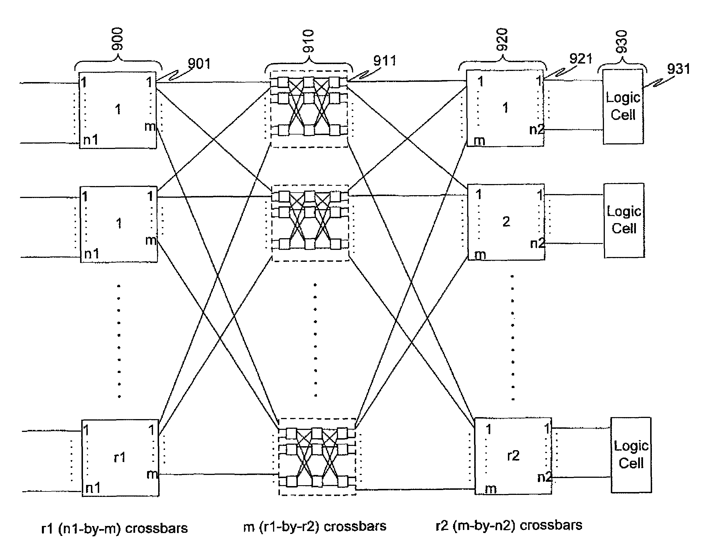
[0052]The present invention provides an area-efficient and highly routable interconnect scheme for use in a programmable logic device, such as an FPGA, with a cluster-based architecture. This interconnect scheme may be used as an internal cluster routing network to provide routing for signals to be input to logic cells, such as look-up tables (LUTs), in the clusters. The interconnect scheme is a three-stage routing network based on a Clos network architecture.
[0053]The interconnect scheme of the present invention is not a non-blocking network (even for rearrangeably unicast signals) because implementing such an architecture would still have a high cost. Instead, the present invention comprises a blocking Clos network defined by certai...
PUM
 Abstract
Description
Claims
Application Information
 - R&D
- Intellectual Property
- Life Sciences
- Materials
- Tech Scout
- Unparalleled Data Quality
- Higher Quality Content
- 60% Fewer Hallucinations
Browse by: Latest US Patents, China's latest patents, Technical Efficacy Thesaurus, Application Domain, Technology Topic, Popular Technical Reports.
© 2025 PatSnap. All rights reserved.Legal|Privacy policy|Modern Slavery Act Transparency Statement|Sitemap|About US| Contact US: help@patsnap.com