How To Maximize Tungsten Conductivity In Circuits?
Tungsten Conductivity Enhancement: Background and Objectives
Tungsten has long been recognized as a critical material in the electronics industry, particularly for its use in integrated circuits. Its high melting point, excellent thermal stability, and resistance to electromigration make it an ideal candidate for various applications in microelectronics. However, as the demand for faster and more efficient circuits continues to grow, there is an increasing need to maximize the conductivity of tungsten in these applications.
The evolution of tungsten usage in circuits can be traced back to the early days of semiconductor manufacturing. Initially, aluminum was the primary metal used for interconnects. However, as circuit dimensions shrank and current densities increased, the limitations of aluminum became apparent. This led to the introduction of copper as a replacement, but even copper faced challenges in certain applications, particularly those requiring high temperature stability.
Tungsten emerged as a viable alternative due to its superior thermal properties and resistance to electromigration. Its use in circuits has steadily increased over the years, particularly in areas such as contact plugs, local interconnects, and gate electrodes. The ability of tungsten to withstand high temperatures without degradation has made it especially valuable in power electronics and high-performance computing applications.
Despite its advantages, tungsten's relatively high resistivity compared to copper has been a limiting factor in its widespread adoption. This has led to ongoing research efforts aimed at enhancing tungsten's conductivity while maintaining its other beneficial properties. The primary objective of these efforts is to develop techniques and processes that can significantly reduce the resistivity of tungsten in circuit applications.
Recent advancements in materials science and nanotechnology have opened up new possibilities for tungsten conductivity enhancement. Researchers are exploring various approaches, including alloying, doping, and nanostructuring, to modify the electronic properties of tungsten. These techniques aim to increase the electron mobility within the tungsten structure, thereby improving its overall conductivity.
The goal of maximizing tungsten conductivity in circuits is not only to improve the performance of existing applications but also to enable new possibilities in circuit design. Enhanced conductivity could lead to faster signal propagation, reduced power consumption, and improved thermal management in integrated circuits. This, in turn, could pave the way for more compact and efficient electronic devices across a wide range of industries, from consumer electronics to aerospace and defense.
As we delve deeper into this technical challenge, it is crucial to consider the multifaceted nature of the problem. Enhancing tungsten conductivity involves a complex interplay of material science, electrical engineering, and manufacturing processes. The ultimate aim is to develop practical, scalable solutions that can be integrated into existing semiconductor manufacturing workflows without significant disruption or cost increases.
Market Demand for High-Conductivity Circuit Materials
The demand for high-conductivity circuit materials has been steadily increasing in recent years, driven by the growing need for faster, more efficient, and miniaturized electronic devices. Tungsten, with its excellent thermal and electrical conductivity properties, has emerged as a promising material for advanced circuit applications. The market for high-conductivity materials in the electronics industry is expected to expand significantly over the next decade, with a particular focus on materials that can enhance performance in extreme conditions.
In the semiconductor industry, the push for smaller and more powerful chips has created a strong demand for materials that can efficiently conduct electricity at nanoscale dimensions. Tungsten's ability to maintain its conductivity at very small scales makes it an attractive option for next-generation integrated circuits. This has led to increased interest from major semiconductor manufacturers in incorporating tungsten into their advanced chip designs.
The automotive sector represents another significant market for high-conductivity circuit materials. As electric vehicles become more prevalent, there is a growing need for materials that can handle high power densities and operate reliably under varying temperature conditions. Tungsten's thermal stability and conductivity make it a candidate for use in power electronics and battery management systems in electric vehicles.
Aerospace and defense industries also contribute to the demand for high-conductivity materials like tungsten in circuits. These sectors require components that can withstand extreme environments while maintaining optimal performance. Tungsten's high melting point and resistance to wear make it suitable for use in avionics and other critical systems where reliability is paramount.
The telecommunications industry, particularly with the rollout of 5G and future 6G networks, is another key driver of demand for high-conductivity materials. As data transmission rates increase, the need for materials that can efficiently handle high-frequency signals becomes more critical. Tungsten's properties make it a potential candidate for use in advanced antenna systems and high-frequency circuit components.
In the field of high-performance computing and data centers, the demand for materials that can manage heat dissipation while maintaining high conductivity is growing. Tungsten's thermal conductivity properties could make it valuable in addressing thermal management challenges in densely packed computing environments.
The medical device industry is also showing interest in high-conductivity materials for applications such as implantable devices and diagnostic equipment. Tungsten's biocompatibility and conductivity make it a potential material for advanced medical electronics that require reliable performance within the human body.
As research into quantum computing advances, there is an emerging demand for materials that can maintain superconductivity at higher temperatures. While tungsten itself is not a superconductor, its use in conjunction with other materials in quantum circuits is being explored, potentially opening up new market opportunities in this cutting-edge field.
Current Challenges in Tungsten Conductivity Optimization
Tungsten's high melting point and excellent thermal stability make it an attractive material for circuit applications. However, maximizing its conductivity in circuits presents several significant challenges that researchers and engineers are currently grappling with.
One of the primary obstacles is the inherent resistivity of tungsten, which is higher than that of other commonly used conductive materials like copper or gold. This higher resistivity limits the overall conductivity of tungsten-based circuits, potentially impacting their performance in high-frequency or high-power applications.
Another challenge lies in the formation of tungsten thin films with optimal microstructure. The deposition process of tungsten can result in films with varying grain sizes and orientations, which directly affect the material's electrical properties. Achieving a uniform, fine-grained structure that maximizes conductivity while maintaining other desirable properties is a complex task that requires precise control over deposition parameters.
The integration of tungsten with other materials in circuit fabrication also poses significant challenges. Issues such as adhesion, interfacial reactions, and thermal expansion mismatches can arise when depositing tungsten on various substrates or when combining it with other metals in multilayer structures. These integration challenges can lead to reliability issues and decreased conductivity in the final circuit.
Furthermore, the oxidation of tungsten at elevated temperatures is a critical concern. While tungsten has excellent thermal stability, it can form insulating oxide layers when exposed to oxygen at high temperatures. This oxidation can significantly reduce the conductivity of tungsten interconnects, particularly in applications where circuits operate in harsh environments or at elevated temperatures.
The scaling of tungsten-based interconnects to smaller dimensions, as required by the continued miniaturization of electronic devices, introduces additional conductivity challenges. As the cross-sectional area of tungsten lines decreases, the impact of surface scattering and grain boundary scattering on electron transport becomes more pronounced, potentially leading to increased resistivity at nanoscale dimensions.
Researchers are also facing difficulties in developing effective doping strategies for tungsten to enhance its conductivity. While doping has been successfully used to modify the electrical properties of other materials, finding suitable dopants that can significantly improve tungsten's conductivity without compromising its other beneficial properties remains a challenge.
Lastly, the development of advanced characterization techniques for accurately measuring and analyzing the conductivity of tungsten in complex circuit structures is an ongoing challenge. Existing methods may not provide sufficient resolution or accuracy for optimizing tungsten conductivity at the nanoscale or in intricate three-dimensional circuit architectures.
Existing Methods for Improving Tungsten Conductivity
01 Tungsten-based composite materials for improved conductivity
Composite materials incorporating tungsten are developed to enhance electrical and thermal conductivity. These composites often combine tungsten with other metals or alloys to achieve optimal conductive properties while maintaining other desirable characteristics such as strength and durability.- Tungsten-based composite materials for improved conductivity: Composite materials incorporating tungsten are developed to enhance electrical and thermal conductivity. These composites often combine tungsten with other metals or alloys to achieve optimal conductive properties while maintaining other desirable characteristics such as strength and durability.
- Nanostructured tungsten for enhanced conductivity: Nanostructured forms of tungsten, such as nanowires or nanoparticles, are explored to improve conductivity. These nanostructures can offer increased surface area and unique properties that contribute to enhanced electrical and thermal conduction compared to bulk tungsten.
- Doping and alloying techniques for tungsten conductivity: Various doping and alloying techniques are employed to modify the conductivity of tungsten. By introducing specific elements or compounds into the tungsten matrix, researchers aim to optimize its conductive properties for different applications.
- Surface treatment and coating methods for tungsten conductors: Surface treatments and coating techniques are developed to enhance the conductivity of tungsten-based components. These methods can include chemical treatments, physical vapor deposition, or the application of conductive coatings to improve the overall conductivity of tungsten surfaces.
- Tungsten-based interconnects and wiring for electronic applications: Tungsten and its alloys are utilized in the development of interconnects and wiring for electronic devices. The high conductivity and thermal stability of tungsten make it suitable for applications in integrated circuits and other electronic components where efficient electrical conduction is crucial.
02 Nanostructured tungsten for enhanced conductivity
Nanostructured forms of tungsten, such as nanowires or nanoparticles, are utilized to improve conductivity. These nanostructures can provide increased surface area and unique properties that enhance electrical and thermal conduction in various applications.Expand Specific Solutions03 Tungsten alloys for specific conductivity requirements
Various tungsten alloys are developed to meet specific conductivity requirements in different industries. These alloys may combine tungsten with elements like copper, silver, or other metals to achieve desired conductive properties while maintaining other necessary characteristics.Expand Specific Solutions04 Surface treatment of tungsten for conductivity enhancement
Surface treatments and modifications of tungsten components are employed to enhance conductivity. These treatments may include chemical processes, physical vapor deposition, or other techniques to optimize the surface properties for improved electrical or thermal conduction.Expand Specific Solutions05 Tungsten-based thin films for conductive applications
Thin films containing tungsten are developed for various conductive applications, particularly in electronics and semiconductor industries. These films offer high conductivity while maintaining other necessary properties such as stability and compatibility with other materials in the device structure.Expand Specific Solutions
Key Players in Tungsten Circuit Manufacturing
The maximization of tungsten conductivity in circuits is a critical technological challenge in the mature semiconductor industry. The market for this technology is substantial, driven by the increasing demand for high-performance electronic devices. Companies like Applied Materials, IBM, and Samsung Electronics are at the forefront of developing advanced tungsten-based solutions. The technology's maturity varies, with established players like TSMC and GlobalFoundries focusing on refining existing processes, while newer entrants like Ganzhou Hongfei Tungsten & Molybdenum Materials Co., Ltd. are exploring innovative approaches. The competitive landscape is intense, with both semiconductor manufacturers and materials suppliers vying for technological leadership in this crucial area of circuit design and fabrication.
Applied Materials, Inc.
International Business Machines Corp.
Innovative Approaches to Tungsten Conductivity Enhancement
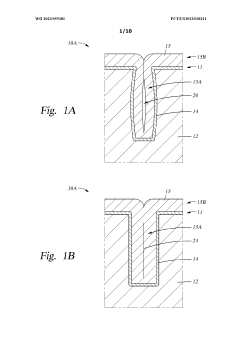
- A method involving the formation of a tungsten-containing layer with a nucleation layer containing boron and tungsten, deposited using a combination of tungsten precursor gases and reducing agents in a cyclic process, followed by an inhibition treatment with activated nitrogen species to create a differential deposition profile, resulting in a seamless and void-free gapfill layer with low resistivity.


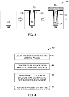
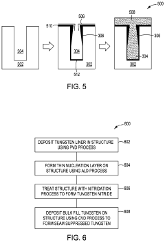
- The proposed method involves a physical vapor deposition of a tungsten liner, followed by an atomic layer deposition nucleation layer and a chemical vapor deposition bulk fill process, with a nitridation step and optional rapid thermal processing to reduce internal stresses and lower resistivity, using argon or krypton as ambient gases and optimizing temperature, pressure, and nitridation conditions.


Environmental Impact of Tungsten Circuit Production
The environmental impact of tungsten circuit production is a critical consideration in the pursuit of maximizing tungsten conductivity in circuits. The extraction and processing of tungsten for use in electronic components have significant ecological implications that must be carefully evaluated and mitigated.
Tungsten mining, the first step in the production chain, can lead to substantial land disturbance and habitat destruction. Open-pit mining, commonly used for tungsten extraction, results in large-scale excavation and the removal of topsoil and vegetation. This process can disrupt local ecosystems, potentially leading to biodiversity loss and altered landscapes.
Water pollution is another major concern associated with tungsten production. The mining and ore processing stages often involve the use of chemicals and generate wastewater containing heavy metals and other contaminants. If not properly managed, these pollutants can seep into groundwater or nearby water bodies, affecting aquatic ecosystems and potentially contaminating drinking water sources for local communities.
Air quality is also impacted by tungsten circuit production. The smelting and refining processes release particulate matter and various gases into the atmosphere. These emissions can contribute to air pollution, potentially affecting human health and contributing to climate change if greenhouse gases are released in significant quantities.
Energy consumption is a substantial factor in the environmental footprint of tungsten circuit production. The entire process, from mining to refining and circuit manufacturing, requires significant amounts of energy. This energy demand often relies on fossil fuel sources, contributing to carbon emissions and exacerbating climate change concerns.
Waste management presents another environmental challenge. The production of tungsten circuits generates various waste streams, including mining tailings, chemical byproducts, and electronic waste from discarded or obsolete circuits. Proper disposal and recycling of these materials are essential to prevent soil and water contamination and reduce the overall environmental impact.
To address these environmental concerns, the industry is increasingly focusing on sustainable practices. These include implementing more efficient extraction techniques, developing closed-loop water systems to minimize water consumption and pollution, and investing in cleaner energy sources for production facilities. Additionally, efforts are being made to improve recycling processes for tungsten-containing products, which can reduce the need for new mining activities and decrease the overall environmental footprint of tungsten circuit production.
As research continues on maximizing tungsten conductivity in circuits, it is crucial to consider these environmental factors. Balancing technological advancements with ecological responsibility will be key to ensuring the sustainable development of tungsten-based circuit technologies.
Thermal Management in High-Conductivity Tungsten Circuits
Thermal management is a critical aspect of maximizing tungsten conductivity in circuits, particularly as the demand for high-performance electronic devices continues to grow. The high thermal conductivity of tungsten, coupled with its excellent electrical properties, makes it an ideal candidate for use in advanced circuit designs. However, as circuit densities increase and power requirements escalate, managing heat dissipation becomes increasingly challenging.
One of the primary approaches to thermal management in high-conductivity tungsten circuits involves the implementation of advanced heat spreading techniques. These methods aim to distribute heat more evenly across the circuit, preventing the formation of localized hot spots that can degrade performance and reliability. Thin-film tungsten heat spreaders, for instance, can be integrated into the circuit design to efficiently conduct heat away from critical components.
Another key strategy is the optimization of circuit layout and component placement. By carefully arranging tungsten interconnects and other circuit elements, designers can minimize thermal resistance and improve overall heat dissipation. This may involve the use of computational fluid dynamics (CFD) simulations to model heat flow and identify potential thermal bottlenecks before physical prototyping.
The integration of micro-channel cooling systems represents a more advanced approach to thermal management in tungsten circuits. These systems involve the fabrication of microscale channels within the tungsten substrate, through which coolant can be circulated to actively remove heat. The high thermal conductivity of tungsten facilitates efficient heat transfer from the circuit to the coolant, enabling more effective temperature control.
Emerging technologies such as phase-change materials (PCMs) are also being explored for their potential in managing thermal issues in high-conductivity tungsten circuits. PCMs can absorb and release large amounts of latent heat during phase transitions, providing a buffer against temperature spikes and helping to maintain more stable operating conditions.
Furthermore, the development of novel packaging solutions plays a crucial role in thermal management. Advanced thermal interface materials (TIMs) can be used to improve heat transfer between the tungsten circuit and external heat sinks or cooling systems. These materials are designed to fill microscopic air gaps and enhance thermal conductivity across interfaces, thereby reducing overall thermal resistance.
As the push for higher performance and miniaturization continues, researchers are also investigating the potential of three-dimensional integrated circuits (3D ICs) incorporating tungsten. This approach presents new challenges and opportunities for thermal management, requiring innovative cooling solutions such as through-silicon vias (TSVs) filled with high-conductivity materials like tungsten to facilitate vertical heat dissipation.