Electrical contact
- Summary
- Abstract
- Description
- Claims
- Application Information
AI Technical Summary
Benefits of technology
Problems solved by technology
Method used
Image

Examples
Embodiment Construction
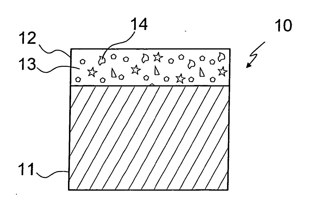
[0033]FIG. 1 schematically illustrates a surface of an electric contact 10, which is a contact of a plug-in connector for use in an automobile.
[0034] Electric contact 10 includes a substrate 11 which is manufactured from a copper-based alloy such as CuSn4, CuNi2Si or the like. Substrate 11 has a thickness of between 0.1 mm and 0.5 mm.
[0035] A contact layer 12 is applied to substrate 11 by an electrolytic method. Contact layer 12 has a layer thickness of between approximately 1 μm and 3 μm and has a matrix 13 made of tin. Hard particles 14 of aluminum oxide Al2O3 having a particle size of between 20 nm and 200 nm are distributed, i.e., “dispersed,” in matrix 13. Contact layer 12 thus represents a solid-state nanodispersion.
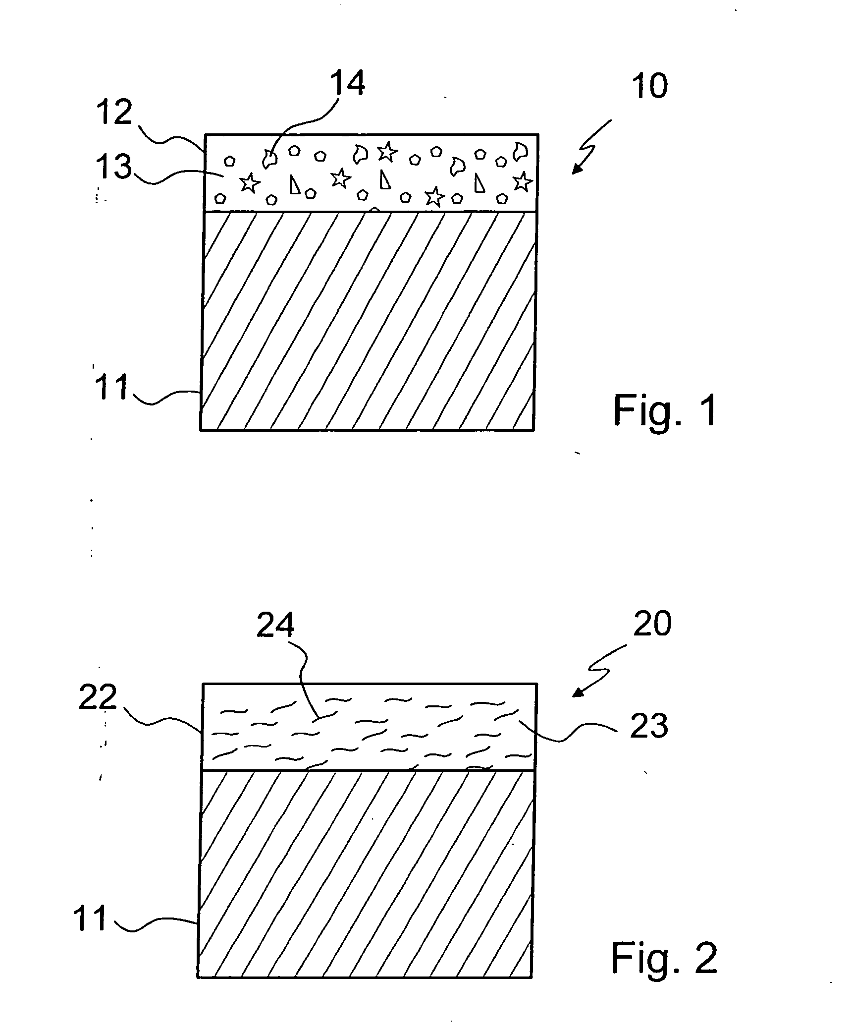
[0036]FIG. 2 schematically illustrates an electric contact 20, which is also a contact of a plug-in connector for use in an automobile.
[0037] Similar to the electric contact of FIG. 1, electric contact 20 includes a substrate 11 which is made of a copper-based ...
PUM
| Property | Measurement | Unit |
|---|---|---|
| Size | aaaaa | aaaaa |
| Size | aaaaa | aaaaa |
| Dispersion potential | aaaaa | aaaaa |
Abstract
Description
Claims
Application Information
 - R&D
- Intellectual Property
- Life Sciences
- Materials
- Tech Scout
- Unparalleled Data Quality
- Higher Quality Content
- 60% Fewer Hallucinations
Browse by: Latest US Patents, China's latest patents, Technical Efficacy Thesaurus, Application Domain, Technology Topic, Popular Technical Reports.
© 2025 PatSnap. All rights reserved.Legal|Privacy policy|Modern Slavery Act Transparency Statement|Sitemap|About US| Contact US: help@patsnap.com