Front electrode for use in photovoltaic device and method of making same
- Summary
- Abstract
- Description
- Claims
- Application Information
AI Technical Summary
Benefits of technology
Problems solved by technology
Method used
Image

Examples
example 1
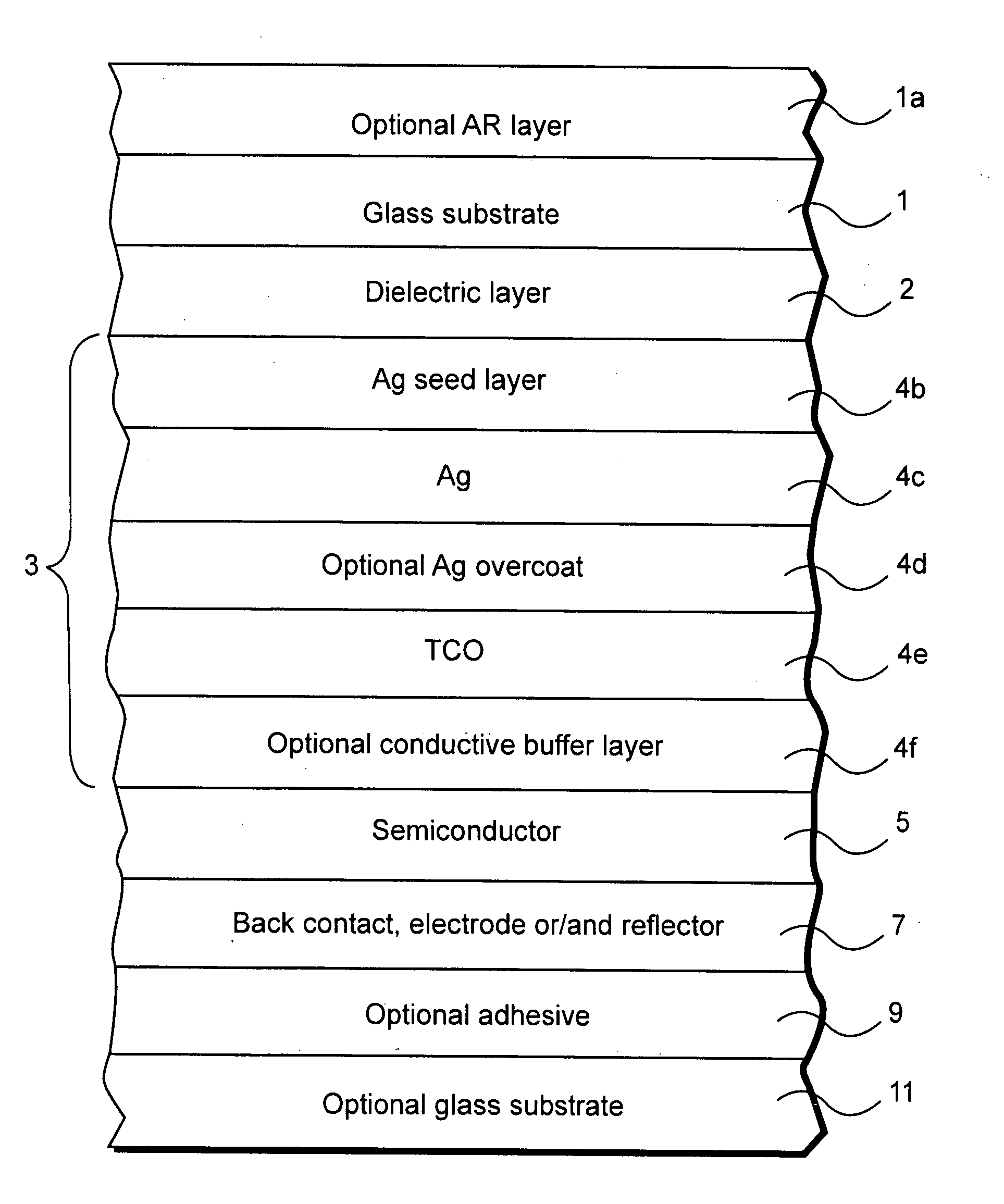
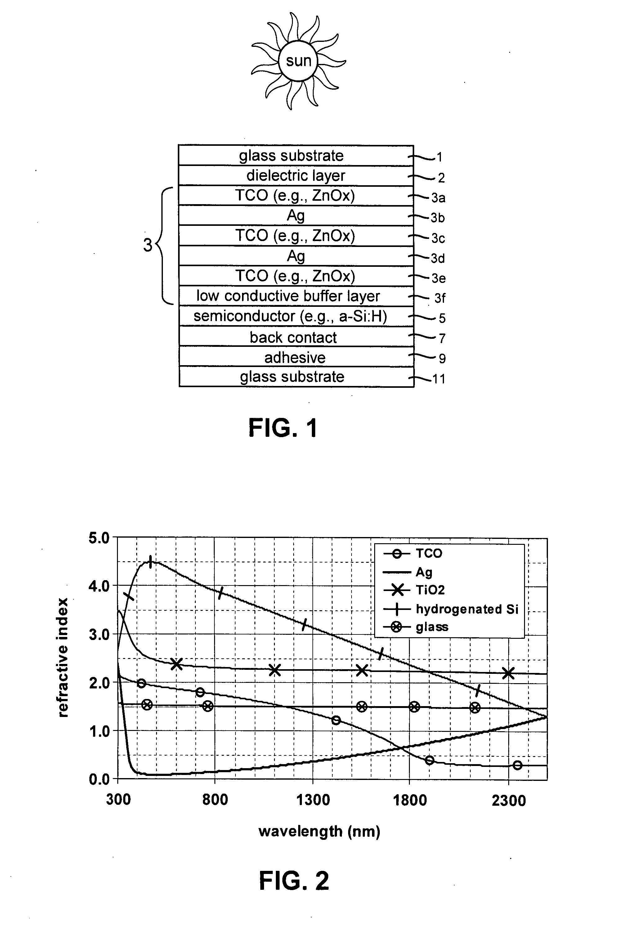
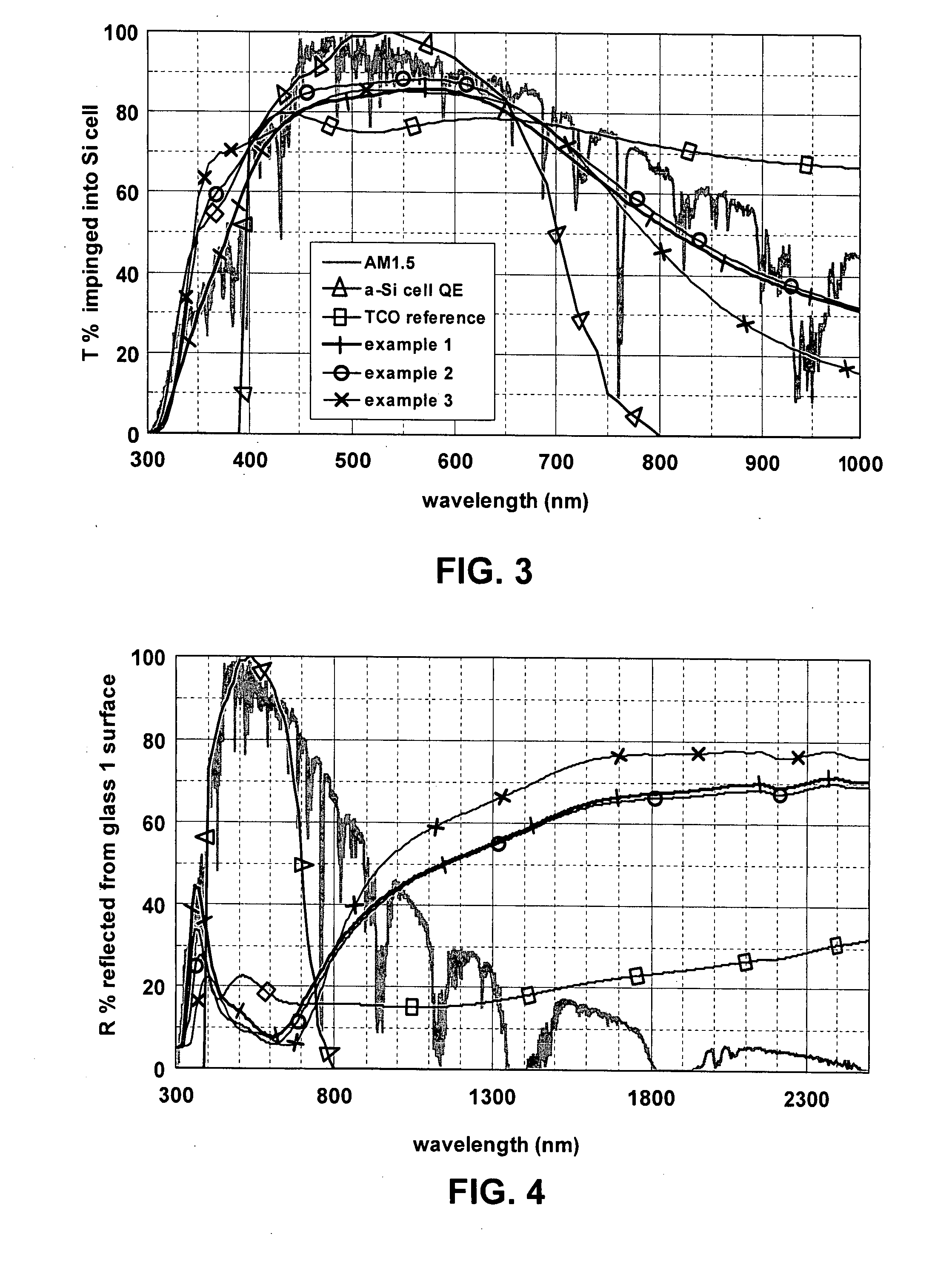
[0040]Example 1 shown in FIG. 5 and charted in FIGS. 3-4 was made up of 3 mm thick glass substrate 1, 16 nm thick TiO2 dielectric layer 2, 10 nm thick zinc oxide TCO doped with Al 3a, 8 nm thick Ag IR reflecting layer 3b, and 115 nm thick zinc oxide TCO doped with Al 3e. Layers 3c, 3d and 3f were not present in Example 2 shown in FIG. 6 and charted in FIGS. 3-4 was made up of 3 mm thick glass substrate 1, 16 nm thick TiO2 dielectric layer 2, 10 nm thick zinc oxide TCO doped with Al 3a, 8 nm thick Ag IR reflecting layer 3b, 100 nm thick zinc oxide TCO doped with Al 3e, and 20 nm thick titanium suboxide layer 3f. Example 3 shown in FIG. 7 and charted in FIGS. 3-4 was made up of 3 mm thick glass substrate 1, 45 nm thick dielectric layer 2, 10 nm thick zinc oxide TCO doped with Al 3a, 5 nm thick Ag IR reflecting layer 3b, 75 nm thick zinc oxide TCO doped with Al 3c, 7 nm thick Ag IR reflecting layer 3d, 95 nm thick zinc oxide TCO doped with Al 3e, and 20 nm thick titanium suboxide laye...
PUM
 Abstract
Description
Claims
Application Information
 - R&D
- Intellectual Property
- Life Sciences
- Materials
- Tech Scout
- Unparalleled Data Quality
- Higher Quality Content
- 60% Fewer Hallucinations
Browse by: Latest US Patents, China's latest patents, Technical Efficacy Thesaurus, Application Domain, Technology Topic, Popular Technical Reports.
© 2025 PatSnap. All rights reserved.Legal|Privacy policy|Modern Slavery Act Transparency Statement|Sitemap|About US| Contact US: help@patsnap.com