Cable for high-voltage electronic device
- Summary
- Abstract
- Description
- Claims
- Application Information
AI Technical Summary
Benefits of technology
Problems solved by technology
Method used
Image

Examples
example 1
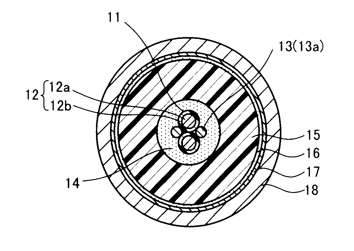
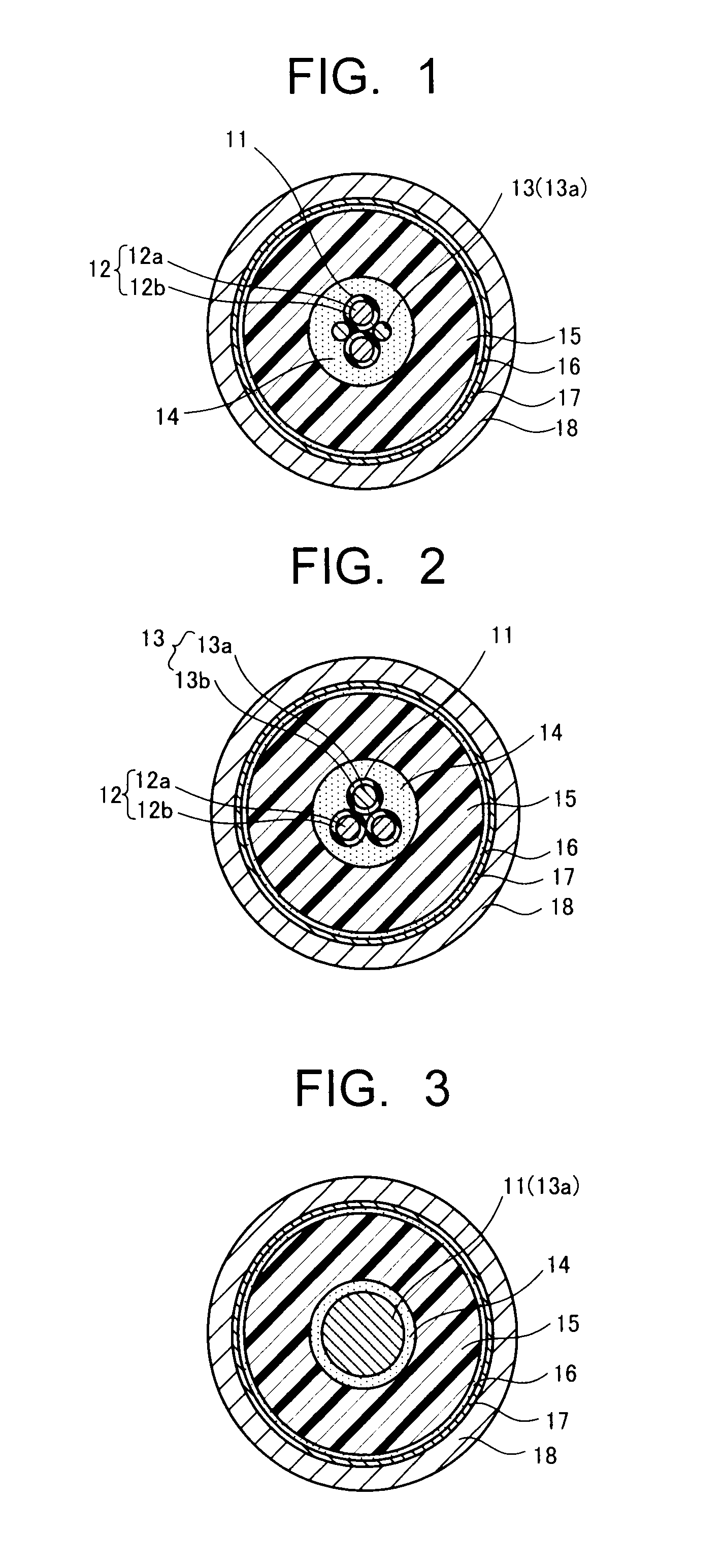
[0035]On a conductor having a cross-sectional area of 1.8 mm2 which was formed by concentric stranding of 19 tin-coated annealed copper wires having a diameter of 0.35 mm, two lines of low-voltage cable cores having an insulator formed of polytetrafluoroethylene and having a thickness of 0.25 mm and two lines of high-voltage cable cores composed of a bare conductor having a cross-sectional area of 1.25 mm2 which was formed by concentric stranding of 50 tin-coated annealed copper wires having a diameter of 0.18 mm were stranded, and then a semiconductive tape formed of a nylon substrate was wound around the outer periphery to form an inner semiconducting layer having a thickness of about 0.5 mm.
[0036]An insulating composition, which was prepared by homogeneously kneading 100 parts by mass of EPDM (Mitsui EPT #1045, trade name, manufactured by Mitsui Chemicals, Inc.), 0.5 part by mass of fumed silica (AEROSIL 300, trade name, manufactured by Nippon Aerosil Co., Ltd.) and 2.5 parts by ...
PUM
| Property | Measurement | Unit |
|---|---|---|
| Length | aaaaa | aaaaa |
| Percent by mass | aaaaa | aaaaa |
| Percent by mass | aaaaa | aaaaa |
Abstract
Description
Claims
Application Information
 - R&D
- Intellectual Property
- Life Sciences
- Materials
- Tech Scout
- Unparalleled Data Quality
- Higher Quality Content
- 60% Fewer Hallucinations
Browse by: Latest US Patents, China's latest patents, Technical Efficacy Thesaurus, Application Domain, Technology Topic, Popular Technical Reports.
© 2025 PatSnap. All rights reserved.Legal|Privacy policy|Modern Slavery Act Transparency Statement|Sitemap|About US| Contact US: help@patsnap.com