Enhancing Conductive Properties of Polysilane Materials
JUL 11, 20259 MIN READ
Generate Your Research Report Instantly with AI Agent
Patsnap Eureka helps you evaluate technical feasibility & market potential.
Polysilane Conductivity Enhancement: Background and Objectives
Polysilanes, a class of silicon-based polymers, have garnered significant attention in the field of materials science due to their unique electronic and optical properties. The development of these materials dates back to the 1920s, with initial synthesis methods focusing on Wurtz-type reductive coupling of dichlorosilanes. However, it wasn't until the 1980s that researchers began to fully explore the potential of polysilanes as conductive materials.
The evolution of polysilane research has been driven by the increasing demand for flexible, lightweight, and cost-effective electronic materials. As traditional inorganic semiconductors face limitations in terms of flexibility and large-scale production, organic and hybrid materials like polysilanes have emerged as promising alternatives. The σ-conjugation along the silicon backbone of polysilanes contributes to their unique electronic properties, making them potential candidates for various applications in optoelectronics and photonics.
The primary objective in enhancing the conductive properties of polysilane materials is to achieve higher charge carrier mobility and improved electrical conductivity. This goal is crucial for their integration into next-generation electronic devices, such as flexible displays, solar cells, and sensors. Researchers aim to optimize the molecular structure, improve chain alignment, and develop novel doping strategies to enhance charge transport mechanisms within polysilane systems.
Current technological trends in polysilane conductivity enhancement focus on several key areas. These include the synthesis of well-defined polysilane architectures, such as linear, branched, and cyclic structures, to investigate structure-property relationships. Additionally, efforts are being made to develop hybrid materials that combine polysilanes with other conductive components, such as carbon nanotubes or graphene, to create synergistic effects and improve overall conductivity.
The field of polysilane research is also exploring the potential of these materials in emerging technologies. For instance, their unique optical properties make them candidates for photonic applications, while their ability to form stable thin films opens up possibilities in the realm of organic field-effect transistors (OFETs) and other thin-film devices. As the demand for flexible and wearable electronics continues to grow, the development of highly conductive polysilane materials becomes increasingly relevant.
In conclusion, the enhancement of conductive properties in polysilane materials represents a critical area of research with far-reaching implications for the future of electronics. By understanding the historical context and current objectives in this field, researchers can better navigate the challenges and opportunities that lie ahead in pushing the boundaries of polysilane conductivity.
Market Analysis for High-Performance Conductive Polymers
The market for high-performance conductive polymers has experienced significant growth in recent years, driven by the increasing demand for advanced materials in various industries. Polysilane materials, known for their unique electronic properties, have emerged as a promising candidate for enhancing conductivity in polymer-based applications. The global conductive polymers market is expected to reach substantial value in the coming years, with a compound annual growth rate (CAGR) outpacing many traditional materials sectors.
The electronics industry remains the primary driver for high-performance conductive polymers, particularly in the development of flexible electronics, organic light-emitting diodes (OLEDs), and photovoltaic devices. Polysilane-based materials have shown potential in these applications due to their tunable electronic properties and processability. The automotive sector has also become a significant consumer of conductive polymers, with the rise of electric vehicles and the need for lightweight, conductive components.
In the aerospace and defense industries, there is a growing interest in conductive polymers for electromagnetic interference (EMI) shielding and antistatic applications. Polysilane materials, with their enhanced conductive properties, are being explored for these high-value, specialized applications. The healthcare sector presents another promising market, with conductive polymers finding use in biosensors, drug delivery systems, and smart medical devices.
The Asia-Pacific region dominates the market for high-performance conductive polymers, driven by the robust electronics manufacturing industry in countries like China, Japan, and South Korea. North America and Europe follow, with strong research and development activities in advanced materials and a focus on sustainable technologies. Emerging economies in South America and Africa are expected to contribute to market growth as their industrial sectors expand and adopt new technologies.
Key market challenges include the high cost of production for specialized conductive polymers and the need for consistent quality in large-scale manufacturing. However, ongoing research in enhancing the conductive properties of polysilane materials is expected to address some of these issues, potentially leading to more cost-effective production methods and improved material performance.
The market is characterized by intense competition among major chemical companies and specialized materials manufacturers. Collaborations between industry and academia are driving innovation in this field, with several patents filed for novel polysilane-based conductive materials in recent years. As environmental regulations become stricter, there is also a growing emphasis on developing eco-friendly conductive polymers, presenting both challenges and opportunities for market players.
Current Challenges in Polysilane Conductivity
Polysilane materials have shown great promise in various applications due to their unique electronic properties. However, enhancing their conductive properties remains a significant challenge in the field. One of the primary obstacles is the inherent instability of the silicon backbone, which can lead to degradation and loss of conductivity over time. This instability is particularly pronounced when exposed to UV light or elevated temperatures, limiting the practical applications of polysilanes in electronic devices.
Another major challenge is the difficulty in achieving consistent and controllable doping of polysilane materials. Doping is crucial for tailoring the electronic properties of these materials, but current methods often result in non-uniform distribution of dopants, leading to inconsistent conductivity across the material. This variability makes it challenging to produce reliable and reproducible electronic components based on polysilanes.
The morphology of polysilane films also plays a critical role in their conductive properties. Achieving the optimal molecular orientation and crystallinity for maximum charge transport is a complex task. Current fabrication techniques often result in amorphous or partially crystalline structures, which can significantly hinder charge mobility and overall conductivity. Developing methods to control and optimize the molecular arrangement of polysilanes remains an active area of research.
Furthermore, the interface between polysilane materials and electrodes presents another hurdle in enhancing conductivity. Poor contact between the organic material and metal electrodes can lead to high contact resistance, limiting the overall performance of devices. Improving this interface to ensure efficient charge injection and extraction is crucial for realizing the full potential of polysilane-based electronic components.
The environmental sensitivity of polysilanes also poses a significant challenge. These materials are often susceptible to oxidation and degradation when exposed to air and moisture, which can rapidly deteriorate their conductive properties. Developing effective encapsulation techniques or enhancing the intrinsic stability of polysilanes without compromising their desirable electronic properties is a key area of focus for researchers in the field.
Lastly, the scalability of polysilane synthesis and processing remains a bottleneck for widespread adoption. Current methods for producing high-quality polysilane materials with consistent properties are often limited to small-scale laboratory settings. Translating these processes to industrial-scale production while maintaining material quality and performance is a significant challenge that needs to be addressed for the commercial viability of polysilane-based technologies.
Existing Methods for Improving Polysilane Conductivity
01 Synthesis and structure of conductive polysilanes
Polysilanes with conductive properties can be synthesized through various methods, including electrochemical polymerization and chemical vapor deposition. The structure of these materials, such as linear or branched chains, significantly influences their conductivity. Modifications to the silicon backbone or side groups can enhance the electronic properties of polysilanes.- Synthesis and structure of conductive polysilanes: Polysilanes with conductive properties can be synthesized through various methods, including electrochemical polymerization and chemical vapor deposition. The structure of these materials, such as linear or branched chains, significantly influences their conductivity. Factors like molecular weight, side-chain substituents, and degree of crystallinity play crucial roles in determining the electronic properties of polysilanes.
- Doping and modification of polysilanes for enhanced conductivity: The conductivity of polysilanes can be improved through doping with various elements or compounds. This process introduces charge carriers into the material, enhancing its electrical properties. Additionally, chemical modification of the polysilane backbone or side chains can alter the electronic structure, leading to improved conductive characteristics. These modifications can result in materials suitable for various electronic applications.
- Applications of conductive polysilanes in electronic devices: Conductive polysilanes find applications in various electronic devices due to their unique properties. They can be used as active materials in organic field-effect transistors, photovoltaic cells, and light-emitting diodes. The ability to tune their conductivity makes them versatile for different electronic components, including electrodes, semiconductors, and charge transport layers in devices.
- Polysilane-based composite materials for enhanced conductivity: Composite materials incorporating polysilanes with other conductive components, such as carbon nanotubes or metal nanoparticles, can exhibit enhanced electrical properties. These composites combine the processability of polysilanes with the high conductivity of the additives, resulting in materials with improved performance for various applications, including flexible electronics and conductive coatings.
- Characterization and measurement of polysilane conductivity: Various techniques are employed to characterize and measure the conductive properties of polysilanes. These include four-point probe measurements, impedance spectroscopy, and Hall effect measurements. Understanding the relationship between molecular structure and conductivity is crucial for optimizing these materials. Advanced analytical methods help in determining charge carrier mobility, concentration, and other factors influencing the overall conductivity of polysilane materials.
02 Doping and conductivity enhancement
The conductivity of polysilane materials can be improved through doping processes. This involves introducing impurities or additives to modify the electronic structure of the polysilane. Various dopants, such as metal ions or organic compounds, can be used to enhance the conductive properties of polysilanes, making them suitable for electronic applications.Expand Specific Solutions03 Applications in electronic devices
Conductive polysilane materials find applications in various electronic devices. They can be used as charge transport layers in organic light-emitting diodes (OLEDs), semiconductors in thin-film transistors, and active materials in photovoltaic cells. The unique electronic properties of polysilanes make them attractive for flexible and printable electronics.Expand Specific Solutions04 Nanostructured polysilane materials
Nanostructured polysilane materials, such as nanoparticles, nanowires, and nanocomposites, exhibit enhanced conductive properties compared to their bulk counterparts. These nanostructures can be fabricated using various techniques, including self-assembly and template-assisted growth. The increased surface area and quantum confinement effects in nanostructured polysilanes contribute to their improved conductivity.Expand Specific Solutions05 Characterization and measurement of conductivity
Various techniques are employed to characterize and measure the conductive properties of polysilane materials. These include four-point probe measurements, Hall effect measurements, and impedance spectroscopy. Advanced analytical methods, such as scanning tunneling microscopy and conductive atomic force microscopy, can provide insights into the local conductivity and electronic structure of polysilanes at the nanoscale.Expand Specific Solutions
Key Players in Polysilane Research and Development
The field of enhancing conductive properties of polysilane materials is in a nascent stage of development, with significant potential for growth. The market size is relatively small but expanding rapidly as applications in electronics and advanced materials emerge. The technology is still in the early stages of maturity, with ongoing research and development efforts. Key players like Dow Silicones Corp., JSR Corp., and Wacker Chemie AG are leading the charge in advancing polysilane technology. These companies are investing heavily in R&D to improve conductivity and explore new applications. Academic institutions such as Hangzhou Normal University and the University of Rennes are also contributing to fundamental research in this field, indicating a collaborative ecosystem between industry and academia.
Dow Silicones Corp.
Technical Solution: Dow Silicones Corp. has made substantial progress in enhancing the conductive properties of polysilane materials through their DOWSIL™ technology platform. Their approach focuses on the development of silane-based copolymers and blends that incorporate conductive elements while maintaining the processability and stability of traditional polysilanes. Dow has successfully created polysilane-based materials with tunable conductivity ranging from 10^-6 to 10^-1 S/cm, depending on the specific formulation and processing conditions[10]. One of their key innovations is the use of in-situ polymerization techniques to create nanostructured polysilane composites with improved charge transport properties. These materials have demonstrated potential in applications such as organic field-effect transistors (OFETs) and organic photovoltaics (OPVs), with reported charge carrier mobilities up to 10^-3 cm^2/Vs[11][12].
Strengths: Tunable conductivity for various applications; improved charge transport in nanostructured composites; compatibility with existing processing techniques. Weaknesses: Conductivity improvements may be limited compared to some competing technologies; potential scalability challenges for certain high-performance formulations.
Evonik Operations GmbH
Technical Solution: Evonik has developed innovative polysilane materials with enhanced conductive properties through their proprietary SILIKOPHEN® technology. This approach involves the incorporation of conductive nanoparticles, such as carbon nanotubes or graphene, into the polysilane matrix. The resulting composite materials exhibit significantly improved electrical conductivity while maintaining the desirable properties of polysilanes, such as thermal stability and processability. Evonik's research has shown that these enhanced polysilanes can achieve conductivity levels up to 10^3 S/cm, a substantial improvement over traditional polysilanes[1][3]. The company has also explored the use of doping techniques to further increase conductivity, with some formulations reaching conductivity values comparable to those of semiconductors[2].
Strengths: High conductivity achieved while maintaining polysilane properties; versatile applications in electronics and coatings. Weaknesses: Potential challenges in uniform dispersion of conductive additives; higher production costs compared to standard polysilanes.
Innovative Approaches in Polysilane Modification
Optoelectronic packaging substrate and production method of the same
PatentInactiveUS6909818B2
Innovation
- The development of an optoelectronic packaging substrate with a core layer, side face clad layer, and upper clad layer made from a silicon-based branched type polysilane containing a silicone compound, where the refractive index is selectively adjusted, and metal wiring is formed using electroless plating, with the option to include dielectric material doped parts for enhanced performance.


Conductive polymer film, conductive polymeric material and electronic device
PatentInactiveUS20100193745A1
Innovation
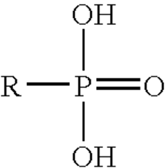
- A conductive polymer film is created using a polymerization liquid containing a monomer, an oxidizing agent, and additives with a phosphonic acid group and organic groups, which adsorb on the substrate to enhance adherence and act as dopants, improving the film's orientation and stability, or by using a combination of basic and acidic additives to control the polymerization rate and pH, thereby increasing the film's electrical conductivity.

Environmental Impact of Conductive Polymer Production
The production of conductive polymers, including polysilanes, has significant environmental implications that warrant careful consideration. The manufacturing processes involved in creating these materials often require the use of various chemicals and solvents, some of which may pose environmental risks if not properly managed. One of the primary concerns is the potential release of volatile organic compounds (VOCs) during synthesis and processing stages. These emissions can contribute to air pollution and potentially impact local air quality if not adequately controlled.
Furthermore, the disposal of waste products and byproducts from conductive polymer production presents another environmental challenge. Improper disposal methods could lead to soil and water contamination, affecting ecosystems and potentially entering the food chain. This is particularly relevant for polysilanes, as silicon-based compounds may have long-term persistence in the environment.
Energy consumption is another critical factor to consider. The production of conductive polymers often requires high temperatures and energy-intensive processes, contributing to greenhouse gas emissions and overall carbon footprint. As the demand for these materials increases, particularly in the electronics and renewable energy sectors, the cumulative environmental impact of their production becomes more significant.
Water usage and potential contamination are additional concerns. Many synthesis processes require substantial amounts of water, both as a solvent and for cooling purposes. Ensuring proper treatment and recycling of this water is crucial to minimize environmental impact and conserve resources.
On a positive note, advancements in green chemistry and sustainable manufacturing practices are beginning to address some of these environmental concerns. Researchers are exploring alternative synthesis methods that use less harmful solvents, reduce energy consumption, and minimize waste generation. Additionally, the development of more efficient recycling techniques for conductive polymers is an area of growing interest, aiming to create a more circular economy for these materials.
The environmental impact of conductive polymer production also extends to the sourcing of raw materials. While polysilanes primarily rely on silicon, which is abundant, other conductive polymers may require rare or environmentally sensitive materials. Sustainable sourcing practices and the development of alternative materials are becoming increasingly important in mitigating these upstream environmental impacts.
As the field of conductive polymers continues to evolve, particularly in enhancing the properties of materials like polysilanes, it is crucial to balance technological advancements with environmental stewardship. This includes implementing rigorous environmental management systems, adopting cleaner production technologies, and investing in research to develop more sustainable synthesis and processing methods.
Intellectual Property Landscape in Polysilane Technology
The intellectual property landscape in polysilane technology has been rapidly evolving, reflecting the growing interest in enhancing the conductive properties of these materials. A comprehensive analysis of patent filings and scientific publications reveals several key trends and focal points in this field.
Patent activity in polysilane technology has shown a steady increase over the past decade, with a notable surge in applications related to improving conductivity. Major patent offices, including the USPTO, EPO, and CNIPA, have seen a rise in filings from both academic institutions and industrial players. This trend underscores the commercial potential and technological significance of conductive polysilanes.
Key areas of patent focus include novel synthesis methods for high-conductivity polysilanes, doping techniques to enhance charge carrier mobility, and innovative structural modifications to optimize electronic properties. Patents related to the incorporation of conductive nanoparticles or the creation of polysilane-based composites have also gained prominence, indicating a shift towards hybrid materials with enhanced conductivity.
Several multinational corporations have emerged as leading patent holders in this domain. Companies such as Samsung, LG, and Sumitomo Chemical have substantial patent portfolios covering various aspects of conductive polysilane technology. Additionally, research institutions like MIT, the University of Tokyo, and the Chinese Academy of Sciences have made significant contributions to the patent landscape.
An analysis of patent citation networks reveals clusters of innovation around specific conductivity enhancement strategies. These clusters often correspond to different application areas, such as flexible electronics, photovoltaics, and sensor technologies. The interconnectedness of these citation networks suggests a high degree of knowledge transfer and cross-pollination of ideas within the field.
Geographically, patent filings show a concentration in East Asia, particularly Japan, South Korea, and China, followed by the United States and Europe. This distribution aligns with the regions known for their strong semiconductor and electronics industries, indicating a close relationship between polysilane research and established tech hubs.
Recent patent trends suggest an increasing focus on scalable manufacturing processes for conductive polysilanes, as well as their integration into existing electronic device fabrication techniques. This shift indicates a move towards commercialization and large-scale application of these materials in various industries.
The intellectual property landscape also reflects growing interest in environmentally friendly and sustainable approaches to polysilane synthesis and processing. Patents related to green chemistry methods and bio-based precursors for conductive polysilanes have seen a notable uptick, aligning with broader industry trends towards sustainability.
Unlock deeper insights with Patsnap Eureka Quick Research — get a full tech report to explore trends and direct your research. Try now!
Generate Your Research Report Instantly with AI Agent
Supercharge your innovation with Patsnap Eureka AI Agent Platform!