Graphene Oxide: Pioneering Thin-Film Transistor Progress
Graphene Oxide TFT Evolution and Objectives
Graphene oxide (GO) has emerged as a groundbreaking material in the field of thin-film transistors (TFTs), marking a significant milestone in the evolution of electronic devices. The journey of GO in TFT technology began with the isolation of graphene in 2004, which sparked intense research into its derivatives. GO, with its unique combination of electrical and mechanical properties, quickly gained attention for its potential in flexible and transparent electronics.
The primary objective in GO TFT development has been to harness its exceptional carrier mobility and atomic thickness to create high-performance, ultra-thin electronic devices. Researchers have focused on overcoming the challenges of GO's inherent insulating nature while preserving its desirable characteristics. This has led to the exploration of various reduction techniques to create reduced graphene oxide (rGO), which exhibits improved conductivity.
Over the past decade, significant progress has been made in optimizing GO TFT performance. Key objectives have included enhancing the on/off current ratio, increasing carrier mobility, and improving overall device stability. These goals have driven innovations in GO synthesis methods, deposition techniques, and device architectures. Researchers have also aimed to develop scalable production processes to facilitate the transition from laboratory prototypes to commercial applications.
The evolution of GO TFTs has been closely tied to advancements in nanomaterial science and thin-film technology. Early efforts focused on understanding the fundamental properties of GO and its behavior in transistor structures. As the field progressed, attention shifted towards engineering GO's electronic properties through chemical and physical modifications. This led to the development of hybrid materials and composite structures that combine GO with other nanomaterials to enhance device performance.
Recent objectives in GO TFT research have expanded to include environmental stability, low-temperature processing, and integration with flexible substrates. These aims reflect the growing demand for wearable and foldable electronics. Additionally, there has been a push towards developing GO TFTs for specific applications, such as biosensors, photodetectors, and memory devices, leveraging GO's unique properties in these specialized fields.
Looking forward, the objectives for GO TFT technology continue to evolve. Researchers are now focusing on achieving room-temperature operation, further miniaturization, and seamless integration with existing semiconductor technologies. There is also a growing emphasis on sustainability, with efforts to develop eco-friendly production methods and explore the potential for biodegradable electronics using GO-based materials.
Market Demand for Advanced TFT Technologies
The demand for advanced thin-film transistor (TFT) technologies has been steadily increasing across various industries, driven by the growing need for high-performance, flexible, and energy-efficient electronic devices. The market for TFTs is experiencing significant growth, particularly in sectors such as display technologies, wearable electronics, and flexible sensors.
In the display industry, there is a strong push towards higher resolution, faster refresh rates, and improved energy efficiency. Advanced TFT technologies, including those based on graphene oxide, are poised to meet these demands by offering superior electron mobility and reduced power consumption compared to traditional amorphous silicon-based TFTs. This trend is evident in the development of next-generation OLED displays and flexible screens for smartphones, tablets, and televisions.
The wearable electronics market is another key driver for advanced TFT technologies. As consumers increasingly adopt smartwatches, fitness trackers, and other wearable devices, there is a growing need for flexible, lightweight, and durable TFTs that can conform to various shapes and withstand repeated bending. Graphene oxide-based TFTs show promise in this area due to their excellent mechanical properties and potential for integration into flexible substrates.
In the field of sensors and Internet of Things (IoT) devices, there is a rising demand for low-power, high-sensitivity TFTs that can be used in a wide range of environmental conditions. Advanced TFT technologies offer the potential for improved performance in gas sensors, biosensors, and touch panels, opening up new applications in healthcare, environmental monitoring, and industrial automation.
The automotive industry is also showing increased interest in advanced TFT technologies for use in heads-up displays, infotainment systems, and smart windows. The ability of graphene oxide-based TFTs to operate at high temperatures and withstand harsh environments makes them particularly attractive for automotive applications.
Furthermore, the emerging field of flexible and printed electronics is creating new opportunities for advanced TFT technologies. The ability to fabricate TFTs on flexible substrates using low-temperature processes is enabling the development of roll-to-roll manufacturing techniques, which could significantly reduce production costs and open up new markets for large-area electronics.
As the demand for miniaturization and integration of electronic components continues to grow, advanced TFT technologies are expected to play a crucial role in the development of system-on-panel solutions, where multiple electronic functions are integrated directly onto the display substrate. This trend is particularly relevant for portable devices and IoT applications, where space and power efficiency are critical factors.
Graphene Oxide TFT State and Challenges
Graphene oxide (GO) has emerged as a promising material for thin-film transistors (TFTs), offering unique properties that could revolutionize electronic devices. However, the current state of GO-based TFTs faces several challenges that hinder their widespread adoption and commercialization.
One of the primary challenges is the inconsistent electrical performance of GO-based TFTs. The conductivity and carrier mobility of GO films can vary significantly depending on the synthesis method, reduction process, and environmental conditions. This variability makes it difficult to achieve reproducible and reliable device performance, which is crucial for large-scale manufacturing and integration into complex electronic systems.
Another significant challenge is the relatively low carrier mobility of GO compared to pristine graphene. While graphene exhibits exceptional carrier mobility, the presence of oxygen-containing functional groups in GO disrupts the sp2 carbon network, leading to reduced conductivity and mobility. Researchers are actively working on developing methods to optimize the reduction process and control the oxygen content to strike a balance between processability and electrical performance.
The stability of GO-based TFTs in ambient conditions remains a concern. GO is sensitive to humidity and temperature fluctuations, which can affect device performance and long-term reliability. Developing effective encapsulation techniques and improving the intrinsic stability of GO films are crucial areas of research to address this challenge.
Scalability and integration with existing semiconductor manufacturing processes pose additional hurdles. While GO can be synthesized in large quantities, achieving uniform and defect-free films over large areas is challenging. Furthermore, integrating GO-based TFTs into conventional silicon-based electronics requires developing compatible fabrication processes and addressing potential issues related to material interfaces and device architectures.
The choice of dielectric materials for GO-based TFTs is another critical aspect that requires optimization. The interaction between GO and the gate dielectric can significantly impact device performance, and finding suitable dielectric materials that provide good interface properties and low leakage currents is an ongoing research focus.
Despite these challenges, significant progress has been made in recent years. Researchers have developed various strategies to improve GO-based TFT performance, including chemical doping, hybrid structures, and novel device architectures. The potential for flexible and transparent electronics using GO-based TFTs continues to drive innovation in this field.
As the research community addresses these challenges, the geographic distribution of GO-based TFT development shows concentrations in Asia, particularly in China and South Korea, as well as in Europe and North America. Collaborative efforts between academic institutions and industry partners are accelerating the pace of innovation and bringing GO-based TFTs closer to practical applications.
Current Graphene Oxide TFT Fabrication Methods
01 Fabrication of graphene oxide thin-film transistors
Methods for fabricating graphene oxide thin-film transistors involve depositing graphene oxide layers on substrates, patterning electrodes, and optimizing device structures. These processes aim to enhance the electrical properties and performance of the transistors, including improved carrier mobility and on/off current ratios.- Fabrication of graphene oxide thin-film transistors: Methods for fabricating graphene oxide thin-film transistors involve depositing graphene oxide layers on substrates, patterning the layers, and incorporating them into transistor structures. These processes may include reduction of graphene oxide to improve electrical properties and the use of various deposition techniques to achieve desired film characteristics.
- Doping and functionalization of graphene oxide for TFTs: Techniques for doping and functionalizing graphene oxide to enhance its properties for use in thin-film transistors. This may include chemical treatments, incorporation of nanoparticles, or other modifications to improve conductivity, carrier mobility, or other electrical characteristics of the graphene oxide layer.
- Integration of graphene oxide TFTs in flexible electronics: Methods for incorporating graphene oxide thin-film transistors into flexible and stretchable electronic devices. This includes techniques for depositing graphene oxide on flexible substrates, ensuring device stability during bending or stretching, and integrating with other flexible electronic components.
- Optimization of graphene oxide TFT performance: Strategies for improving the performance of graphene oxide thin-film transistors, including optimizing channel dimensions, gate dielectric materials, and contact electrodes. This may involve novel device architectures, multi-layer structures, or the use of hybrid materials to enhance transistor characteristics.
- Applications of graphene oxide TFTs: Various applications of graphene oxide thin-film transistors in electronic devices and systems. This includes their use in display technologies, sensors, memory devices, and integrated circuits. The unique properties of graphene oxide enable novel functionalities and improved performance in these applications.
02 Doping and functionalization of graphene oxide
Techniques for doping and functionalizing graphene oxide are employed to modify its electronic properties. This includes introducing various dopants or functional groups to the graphene oxide structure, which can enhance conductivity, tune the bandgap, and improve overall transistor performance.Expand Specific Solutions03 Reduction methods for graphene oxide
Various reduction methods are used to convert graphene oxide to reduced graphene oxide, which exhibits improved electrical conductivity. These methods include thermal, chemical, and electrochemical reduction techniques, each offering different advantages in terms of efficiency and scalability for thin-film transistor applications.Expand Specific Solutions04 Integration of graphene oxide in flexible electronics
Graphene oxide thin-film transistors are integrated into flexible and wearable electronic devices. This involves developing fabrication techniques compatible with flexible substrates and ensuring device stability under mechanical stress, enabling applications in bendable displays and sensors.Expand Specific Solutions05 Hybrid structures with other 2D materials
Graphene oxide is combined with other two-dimensional materials to create hybrid structures for thin-film transistors. These heterostructures can leverage the unique properties of different 2D materials to enhance device performance, such as improved carrier transport or increased on/off ratios.Expand Specific Solutions
Key Players in Graphene Oxide TFT Research
The graphene oxide thin-film transistor market is in its early growth stage, characterized by rapid technological advancements and increasing research activities. Major players like Samsung Display, LG Display, and BOE Technology Group are investing heavily in this field, driving market expansion. The global market size for graphene-based electronics is projected to grow significantly in the coming years. While the technology shows promise, it is still evolving, with varying levels of maturity across different applications. Companies such as Global Graphene Group and Nanotek Instruments are focusing on improving manufacturing processes and scalability. Academic institutions like Northwestern University and Tsinghua University are contributing to fundamental research, pushing the boundaries of graphene oxide's potential in thin-film transistors. The competitive landscape is dynamic, with both established electronics manufacturers and specialized graphene companies vying for market share.
Global Graphene Group, Inc.
Semiconductor Energy Laboratory Co., Ltd.
Breakthrough Patents in Graphene Oxide TFTs
- A thin film transistor is developed using graphene for the gate, source, and drain electrodes, with an active region composed of doped oxidized graphene, and a gate insulating layer made of oxidized graphene, reducing oxidized graphene to form these components, which simplifies the production process and enhances electrical conductivity and mobility.
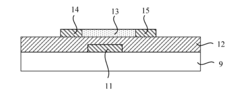
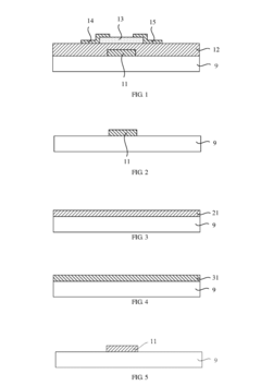

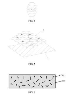
- A thin-film transistor with an active layer composed of a mixture of oxide semiconductor and graphene, where the graphene forms a stable framework that protects the channel from etching damage, allowing for the use of graphene micro-sheets distributed in irregular directions to prevent damage during the etching process.


Environmental Impact of Graphene Oxide TFTs
The environmental impact of Graphene Oxide Thin-Film Transistors (TFTs) is a critical consideration as this technology advances. While graphene oxide offers promising benefits for electronic devices, its production and disposal processes require careful examination to ensure sustainability.
The manufacturing of graphene oxide TFTs involves chemical processes that may generate hazardous waste. The oxidation of graphite to produce graphene oxide often utilizes strong acids and oxidants, which can lead to the release of toxic byproducts if not properly managed. Additionally, the use of solvents in the fabrication process may contribute to air and water pollution if appropriate containment measures are not implemented.
However, the thin-film nature of these transistors means that they require significantly less material compared to traditional silicon-based electronics. This reduction in material usage could potentially lead to a decrease in overall resource consumption and associated environmental impacts in the long term.
The energy efficiency of graphene oxide TFTs is another important factor to consider. These devices have the potential to operate at lower voltages than conventional transistors, which could translate to reduced energy consumption in electronic devices. This improved energy efficiency may contribute to a decrease in the carbon footprint associated with the use of electronic products.
End-of-life considerations for graphene oxide TFTs are also crucial. The recyclability and biodegradability of these devices are areas that require further research. While graphene oxide itself is not inherently toxic, the presence of other materials in the TFT structure may complicate recycling efforts. Developing effective recycling methods for these devices will be essential to minimize electronic waste and recover valuable materials.
The potential for graphene oxide to leach into the environment during the disposal of electronic devices is another concern that needs to be addressed. Studies on the long-term environmental fate and potential ecological impacts of graphene oxide are ongoing, and their findings will be crucial in developing appropriate disposal and recycling strategies.
On a positive note, the durability and flexibility of graphene oxide TFTs may lead to longer-lasting electronic devices, potentially reducing the frequency of device replacement and associated electronic waste generation. This longevity could have a significant positive impact on the overall environmental footprint of consumer electronics.
Scalability and Mass Production Prospects
The scalability and mass production prospects of graphene oxide-based thin-film transistors (TFTs) represent a critical factor in their potential for widespread adoption and commercial viability. As research progresses, significant advancements have been made in developing scalable production methods for graphene oxide (GO) and its integration into TFT devices.
One of the primary challenges in scaling up GO-TFT production lies in the synthesis of high-quality, uniform graphene oxide sheets. Solution-based methods, such as modified Hummers' method, have shown promise for large-scale GO production. These techniques allow for the synthesis of GO in bulk quantities, with the potential for continuous production processes. However, maintaining consistency in the oxidation level and sheet size distribution remains a key focus area for optimization.
The deposition of GO films onto substrates presents another crucial aspect of scalability. Techniques such as spin-coating, spray coating, and roll-to-roll processing have demonstrated potential for large-area deposition of GO films. Roll-to-roll processing, in particular, offers a pathway for continuous, high-throughput production of GO-TFTs on flexible substrates, aligning well with the demands of emerging flexible electronics markets.
Reduction of GO to form reduced graphene oxide (rGO) channels in TFTs is another critical step in the manufacturing process. Scalable reduction methods, including thermal annealing and chemical reduction, are being refined to ensure uniform electrical properties across large areas. The development of selective reduction techniques, such as laser scribing or photolithography-assisted reduction, shows promise for patterning rGO channels with high precision on an industrial scale.
Integration of GO-TFTs into complex circuits and systems poses additional challenges for mass production. Advances in printing technologies, including inkjet printing and screen printing of GO-based inks, offer potential solutions for large-scale device integration. These additive manufacturing techniques could enable the production of entire circuits and systems based on GO-TFTs, reducing material waste and production costs.
Despite these advancements, several hurdles remain in the path to mass production. Ensuring consistent device performance across large production batches is crucial. This requires tight control over GO synthesis, deposition, reduction, and device fabrication processes. Additionally, developing robust encapsulation methods to protect GO-TFTs from environmental factors is essential for long-term device stability in commercial applications.
As research continues, the focus on scalability and mass production is likely to intensify. Collaborative efforts between academic institutions and industry partners will be crucial in bridging the gap between laboratory-scale demonstrations and industrial-scale manufacturing. The development of standardized production protocols and quality control measures will play a vital role in establishing GO-TFTs as a viable technology for large-scale commercial applications.