How to Advance Semiconductor Technologies with Graphene Oxide?
Graphene Oxide in Semiconductors: Background and Objectives
Graphene oxide (GO) has emerged as a revolutionary material in the field of semiconductor technologies, offering unprecedented opportunities for advancing electronic devices and systems. The journey of GO in semiconductors began with the isolation of graphene in 2004, which sparked intense research into its derivatives, including GO. This two-dimensional material, composed of a single layer of carbon atoms arranged in a hexagonal lattice with oxygen-containing functional groups, has captured the attention of researchers and industry professionals alike due to its unique properties and potential applications.
The evolution of semiconductor technologies has been driven by the constant pursuit of miniaturization, improved performance, and energy efficiency. As traditional silicon-based technologies approach their physical limits, the integration of novel materials like GO presents a promising avenue for continued progress. GO's exceptional electrical, thermal, and mechanical properties make it an ideal candidate for addressing many of the challenges faced by the semiconductor industry.
The primary objective of incorporating GO into semiconductor technologies is to overcome the limitations of conventional materials and push the boundaries of device performance. Researchers aim to leverage GO's high carrier mobility, tunable bandgap, and excellent thermal conductivity to develop next-generation electronic components. These advancements could lead to faster, more efficient, and more compact devices, ranging from high-speed transistors to advanced sensors and memory elements.
Another crucial goal is to explore GO's potential in flexible and wearable electronics. The material's mechanical flexibility and strength open up new possibilities for creating bendable and stretchable devices, which could revolutionize consumer electronics and medical technologies. Additionally, GO's compatibility with various substrates and its potential for large-scale production make it an attractive option for cost-effective manufacturing processes.
The semiconductor industry is also focusing on harnessing GO's unique properties for enhancing existing technologies. This includes using GO as a complementary material in silicon-based devices to improve their performance, as well as developing hybrid systems that combine the best features of both materials. The ultimate aim is to create a new generation of semiconductor technologies that can meet the growing demands of emerging applications, such as artificial intelligence, Internet of Things (IoT), and 5G communications.
As research in this field progresses, scientists and engineers are working towards overcoming the challenges associated with GO integration, such as controlling its electrical properties and ensuring long-term stability in devices. The path forward involves a multidisciplinary approach, combining expertise from materials science, electrical engineering, and nanotechnology to unlock the full potential of GO in semiconductor applications.
Market Demand for Advanced Semiconductor Materials
The semiconductor industry is experiencing a growing demand for advanced materials that can enhance performance, reduce power consumption, and enable miniaturization of electronic devices. Graphene oxide, a derivative of graphene, has emerged as a promising candidate to meet these requirements. The market for advanced semiconductor materials is driven by the increasing need for high-performance computing, artificial intelligence, 5G networks, and Internet of Things (IoT) devices.
The global semiconductor market is projected to reach significant growth in the coming years, with a substantial portion attributed to advanced materials. Graphene oxide, in particular, is gaining attention due to its unique properties that can potentially revolutionize semiconductor technologies. Its high electrical conductivity, thermal stability, and mechanical strength make it an attractive option for various applications in the semiconductor industry.
One of the key drivers for the demand of graphene oxide in semiconductors is the push for more efficient and faster electronic devices. As traditional silicon-based technologies approach their physical limits, manufacturers are seeking alternative materials to continue the trend of Moore's Law. Graphene oxide offers the potential to create ultra-thin, flexible, and high-performance electronic components that can outperform current silicon-based technologies.
The market demand for graphene oxide in semiconductors is also fueled by the growing need for energy-efficient devices. With the increasing focus on sustainability and reducing carbon footprints, there is a strong push for semiconductors that consume less power while delivering higher performance. Graphene oxide's excellent thermal conductivity and potential for low-power operation align well with these requirements, making it an attractive option for manufacturers looking to develop more energy-efficient products.
Another factor driving the market demand is the potential for graphene oxide to enable new form factors and applications in the semiconductor industry. Its flexibility and thinness open up possibilities for creating bendable and wearable electronics, which are expected to see significant growth in the coming years. This aligns with the increasing consumer demand for smart wearables and flexible displays, further boosting the market potential for graphene oxide-based semiconductor technologies.
The automotive and aerospace industries are also showing interest in graphene oxide for semiconductor applications. As vehicles become more electrified and autonomous, there is a growing need for advanced semiconductor materials that can withstand harsh environments while providing high performance. Graphene oxide's thermal stability and mechanical strength make it a promising candidate for these applications, potentially driving further market growth.
Current State and Challenges in Graphene Oxide Integration
The integration of graphene oxide (GO) into semiconductor technologies has shown significant promise, yet it faces several challenges that hinder its widespread adoption. Currently, the semiconductor industry is exploring GO as a potential material for various applications, including transistors, sensors, and energy storage devices. The unique properties of GO, such as its high electrical conductivity, thermal stability, and mechanical strength, make it an attractive candidate for advancing semiconductor technologies.
One of the primary challenges in GO integration is the lack of precise control over its chemical composition and structure. The oxygen-containing functional groups on GO's surface can vary significantly, affecting its electrical and mechanical properties. This variability makes it difficult to achieve consistent performance across different batches of GO-based semiconductor devices. Researchers are actively working on developing standardized production methods to ensure uniform GO properties.
Another significant hurdle is the scalability of GO production and integration processes. While laboratory-scale experiments have demonstrated promising results, translating these findings into large-scale manufacturing remains a challenge. The semiconductor industry requires highly reproducible and cost-effective production methods, which are currently not fully established for GO-based technologies.
The interface between GO and traditional semiconductor materials poses another challenge. Achieving seamless integration and optimal electrical contact between GO and silicon-based components is crucial for device performance. Researchers are exploring various surface modification techniques and interface engineering approaches to improve the compatibility and enhance charge transfer efficiency.
Stability and reliability issues also present significant obstacles. GO-based devices may experience performance degradation over time due to environmental factors such as humidity and temperature fluctuations. Developing effective encapsulation methods and improving the long-term stability of GO-based components are active areas of research.
Furthermore, the semiconductor industry faces challenges in integrating GO into existing manufacturing processes. Current fabrication techniques may need to be modified or entirely new processes developed to accommodate GO's unique properties. This adaptation requires significant investment in research and development, as well as potential retooling of production facilities.
Lastly, there are concerns regarding the environmental impact and potential health risks associated with GO production and handling. Addressing these issues is crucial for the widespread adoption of GO in semiconductor technologies. Researchers are investigating eco-friendly synthesis methods and developing safety protocols to mitigate potential risks.
Despite these challenges, the potential benefits of GO integration in semiconductor technologies continue to drive research and development efforts. Overcoming these obstacles will require collaborative efforts between academia, industry, and regulatory bodies to establish standardized production methods, improve scalability, enhance device performance, and ensure safety and sustainability.
Existing Solutions for Graphene Oxide in Semiconductors
01 Synthesis and production methods of graphene oxide
Various methods for synthesizing and producing graphene oxide are described, including chemical exfoliation, oxidation of graphite, and reduction processes. These techniques aim to create high-quality graphene oxide with controlled properties for different applications.- Synthesis and production methods of graphene oxide: Various methods for synthesizing and producing graphene oxide are described, including chemical exfoliation, oxidation of graphite, and reduction processes. These techniques aim to create high-quality graphene oxide with controlled properties for different applications.
- Applications of graphene oxide in energy storage devices: Graphene oxide is utilized in energy storage devices such as batteries and supercapacitors. Its unique properties, including high surface area and conductivity, make it an excellent material for improving the performance and efficiency of these devices.
- Functionalization and modification of graphene oxide: Various methods for functionalizing and modifying graphene oxide are explored to enhance its properties and tailor it for specific applications. These modifications can include chemical treatments, doping, and surface modifications to improve its performance in different fields.
- Graphene oxide-based composites and nanocomposites: The development of graphene oxide-based composites and nanocomposites is discussed, combining graphene oxide with other materials to create hybrid structures with enhanced properties. These composites find applications in various fields, including electronics, sensors, and structural materials.
- Characterization and analysis techniques for graphene oxide: Various characterization and analysis techniques are employed to study the properties and structure of graphene oxide. These methods include spectroscopic techniques, microscopy, and other analytical tools to understand the material's composition, morphology, and behavior.
02 Applications of graphene oxide in energy storage devices
Graphene oxide is utilized in energy storage devices such as batteries and supercapacitors. Its unique properties, including high surface area and conductivity, make it an excellent material for improving the performance and efficiency of these devices.Expand Specific Solutions03 Functionalization and modification of graphene oxide
Various methods for functionalizing and modifying graphene oxide are explored to enhance its properties and tailor it for specific applications. These modifications can include chemical treatments, doping, and composite formation with other materials.Expand Specific Solutions04 Graphene oxide in environmental applications
Graphene oxide is used in environmental applications such as water purification, pollutant removal, and environmental sensing. Its high adsorption capacity and chemical properties make it effective for removing contaminants from water and air.Expand Specific Solutions05 Characterization and analysis techniques for graphene oxide
Various characterization and analysis techniques are employed to study the properties and structure of graphene oxide. These methods include spectroscopic techniques, microscopy, and other analytical tools to determine the quality, composition, and characteristics of graphene oxide materials.Expand Specific Solutions
Key Players in Graphene Oxide Semiconductor Research
The semiconductor industry is in a mature phase, but graphene oxide technology represents an emerging frontier with significant potential for advancement. The global market for graphene-based semiconductors is projected to grow rapidly, driven by demand for high-performance electronics. While the technology is still in early stages of development, several key players are making notable progress. Companies like IBM, Samsung, and Applied Materials are leveraging their extensive semiconductor expertise to explore graphene oxide applications. Startups such as Archer Materials and Paragraf are focusing specifically on graphene-based semiconductor solutions. Academic institutions like Caltech and the University of North Carolina are contributing fundamental research. The technology's maturity varies across applications, with some areas nearing commercialization while others remain in experimental stages.
International Business Machines Corp.
Applied Materials, Inc.
Core Innovations in Graphene Oxide Semiconductor Applications
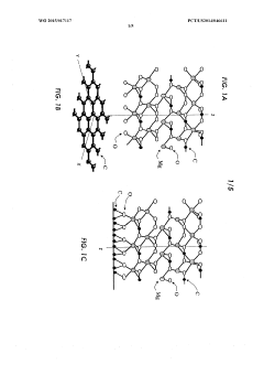
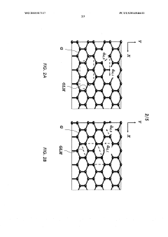
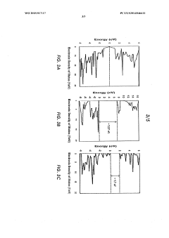
- Forming a semiconducting graphene structure by bonding a graphene-lattice matching material, such as magnesium carbonate, with a lattice constant within ±5% of graphene's, to modify the energy band gap and achieve crystalline alignment, thereby increasing the band gap from zero to approximately 1.7 eV, suitable for semiconductor devices.
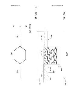
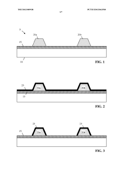
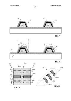
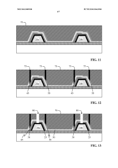
- A method of forming a graphene FET on a sacrificial seed material arranged on the sidewalls of a mandrel, where the graphene is grown using chemical vapor deposition (CVD) and the sacrificial material is subsequently removed, allowing for the formation of a vertical graphene FET without transfer processes, thereby reducing manufacturing complexity and cost.

Environmental Impact of Graphene Oxide Production
The production of graphene oxide, while promising for semiconductor technologies, raises significant environmental concerns that warrant careful consideration. The synthesis process typically involves the oxidation of graphite using strong oxidizing agents, such as potassium permanganate and sulfuric acid, which can lead to the generation of hazardous waste and potentially toxic by-products.
One of the primary environmental impacts is the release of greenhouse gases during the production process. The chemical reactions involved in graphene oxide synthesis can emit carbon dioxide and other greenhouse gases, contributing to global warming and climate change. Additionally, the use of strong acids and oxidizing agents poses risks of soil and water contamination if not properly managed and disposed of.
Water consumption is another critical environmental factor in graphene oxide production. The process requires substantial amounts of water for washing and purification steps, potentially straining local water resources in areas of production. Furthermore, the wastewater generated during these processes may contain residual chemicals and nanomaterials, necessitating advanced treatment methods to prevent environmental contamination.
The production of graphene oxide also raises concerns about resource depletion. While graphite, the primary raw material, is relatively abundant, the increasing demand for graphene-based materials could lead to intensified mining activities, resulting in habitat destruction and ecosystem disruption in graphite-rich regions.
Occupational health and safety issues are closely tied to environmental impacts. The handling of nanomaterials and hazardous chemicals during production poses potential risks to workers and nearby communities through inhalation or dermal exposure. Proper safety protocols and protective equipment are essential to mitigate these risks.
As the scale of graphene oxide production increases to meet growing demand in semiconductor technologies, the cumulative environmental impact becomes more significant. This necessitates the development of greener synthesis methods, such as electrochemical exfoliation or biomass-derived precursors, which could reduce the reliance on harsh chemicals and minimize waste generation.
Lifecycle assessment studies are crucial for comprehensively evaluating the environmental footprint of graphene oxide production. These assessments can help identify hotspots in the production process where environmental impacts are most severe, guiding efforts to improve sustainability. Furthermore, exploring circular economy approaches, such as recycling and reusing graphene oxide materials, could help mitigate long-term environmental consequences.
Intellectual Property Landscape in Graphene Oxide Semiconductors
The intellectual property landscape in graphene oxide semiconductors is rapidly evolving, reflecting the growing interest and potential of this innovative material in advancing semiconductor technologies. Patent filings in this domain have seen a significant increase over the past decade, with major technology companies, research institutions, and startups actively contributing to the expansion of the IP portfolio.
Key areas of patent activity include methods for synthesizing high-quality graphene oxide, techniques for integrating graphene oxide into semiconductor devices, and novel applications leveraging the unique properties of graphene oxide in electronic and optoelectronic components. A notable trend is the focus on developing scalable production methods for graphene oxide, addressing one of the primary challenges in commercializing this technology.
Several leading semiconductor manufacturers have established strong patent positions in graphene oxide-based transistors and memory devices. These patents often cover specific device architectures, fabrication processes, and methods for enhancing the electrical properties of graphene oxide in semiconductor applications. Additionally, there is a growing number of patents related to graphene oxide's use in flexible and wearable electronics, highlighting its potential in emerging market segments.
Universities and research institutions play a crucial role in the IP landscape, often holding foundational patents on graphene oxide synthesis and characterization techniques. Collaborations between academic institutions and industry partners have resulted in joint patent filings, accelerating the transition from laboratory discoveries to practical applications.
The geographical distribution of patent filings shows a concentration in countries with strong semiconductor industries, such as the United States, China, South Korea, and Japan. However, there is an increasing trend of patent applications from emerging economies, indicating a global interest in graphene oxide semiconductor technologies.
Recent patent trends suggest a shift towards more application-specific innovations, with a focus on integrating graphene oxide into existing semiconductor manufacturing processes. This includes patents on methods for depositing graphene oxide layers with precise thickness control, techniques for patterning graphene oxide at the nanoscale, and approaches for modifying its electronic properties through chemical functionalization.
As the field matures, we are likely to see an increase in patent litigation and licensing activities. Companies with strong IP portfolios in graphene oxide semiconductors may gain significant competitive advantages, potentially shaping the future direction of the industry. The complex and interconnected nature of the IP landscape underscores the importance of comprehensive patent strategies for companies looking to leverage graphene oxide in advancing semiconductor technologies.