Comparison of Semiconductor Materials in Bioelectronic Interfaces
OCT 15, 202510 MIN READ
Generate Your Research Report Instantly with AI Agent
Patsnap Eureka helps you evaluate technical feasibility & market potential.
Bioelectronic Interface Materials Evolution and Objectives
The evolution of bioelectronic interfaces has witnessed significant transformations since the early experiments with metal electrodes in the 1950s. Initially, these interfaces primarily utilized noble metals such as gold and platinum due to their biocompatibility and electrical conductivity. However, these materials presented limitations in terms of flexibility, long-term stability, and signal-to-noise ratio when interfacing with biological tissues.
The 1970s marked a pivotal shift with the introduction of silicon-based semiconductor materials in bioelectronic applications. Silicon offered superior electrical properties and manufacturing scalability through established microelectronic fabrication techniques. This period saw the development of the first silicon-based neural probes and biosensors, establishing semiconductors as essential components in bioelectronic interfaces.
The 1990s to early 2000s witnessed the emergence of compound semiconductors such as gallium arsenide (GaAs) and gallium nitride (GaN), offering enhanced optoelectronic properties crucial for applications requiring light emission or detection within biological environments. Concurrently, research into organic semiconductors began gaining momentum, promising improved mechanical compatibility with soft biological tissues.
The past decade has been characterized by rapid diversification in semiconductor materials for bioelectronics. Silicon carbide (SiC) has gained attention for its exceptional biocompatibility and stability in harsh physiological environments. Diamond-based semiconductors have demonstrated remarkable chemical inertness and wide electrochemical windows. Two-dimensional materials like graphene and transition metal dichalcogenides (TMDs) have revolutionized the field with their atomic thinness, flexibility, and unique electronic properties.
The primary objective in bioelectronic interface material development is achieving seamless integration between electronic systems and biological entities. This requires materials that can effectively transduce between ionic signals in biological systems and electronic signals in devices while maintaining long-term stability in physiological environments. Additionally, materials must exhibit minimal foreign body response, appropriate mechanical properties matching biological tissues, and efficient charge transfer capabilities.
Future objectives include developing semiconductor materials with programmable biodegradability for temporary implants, self-healing properties to extend device longevity, and biomimetic functionalities that can adapt to changing physiological conditions. The ultimate goal remains creating truly symbiotic interfaces between electronic systems and biological organisms, enabling applications ranging from advanced neural prosthetics to closed-loop therapeutic systems and high-resolution biosensing platforms.
Market Analysis for Semiconductor-Based Bioelectronic Devices
The global market for semiconductor-based bioelectronic devices is experiencing unprecedented growth, driven by increasing applications in healthcare monitoring, neural interfaces, and implantable medical devices. Current market valuations indicate that the bioelectronic medicine sector reached approximately 19 billion USD in 2022, with projections suggesting a compound annual growth rate of 13.2% through 2030. This robust growth trajectory is supported by increasing investments in healthcare technology and rising prevalence of chronic conditions requiring continuous monitoring.
Demand analysis reveals several key market segments where semiconductor-based bioelectronic interfaces are gaining significant traction. The neural interface segment currently represents the largest market share at 32%, followed by cardiac monitoring devices at 28% and glucose monitoring systems at 21%. Emerging applications in pain management and inflammatory disease treatment are showing the highest growth rates, expanding at over 15% annually.
Regional market assessment indicates North America maintains leadership with approximately 42% market share, attributed to advanced healthcare infrastructure and substantial R&D investments. Asia-Pacific represents the fastest-growing region with 16.5% annual growth, driven by expanding healthcare access in China and India, coupled with strong semiconductor manufacturing capabilities in Taiwan, South Korea, and Japan.
Consumer adoption patterns demonstrate increasing acceptance of bioelectronic devices, with patient satisfaction rates exceeding 75% for non-invasive monitoring solutions. However, market penetration for implantable devices remains relatively low at 12%, primarily due to cost barriers and regulatory hurdles.
Pricing analysis shows significant variation across device categories, with advanced neural interfaces commanding premium prices between 25,000-75,000 USD, while consumer-grade biomonitoring devices typically range from 100-500 USD. Insurance coverage remains a critical factor influencing market adoption, with approximately 60% of advanced bioelectronic treatments receiving partial reimbursement in developed markets.
Regulatory landscape assessment reveals varying approval timelines across regions, with FDA approval processes averaging 3-5 years for implantable semiconductor-based devices. The European market demonstrates a more streamlined approach through CE marking, while Asian markets show considerable regulatory heterogeneity.
Market barriers include high development costs, stringent biocompatibility requirements, and technical challenges in long-term stability of semiconductor materials in biological environments. Despite these challenges, venture capital funding in bioelectronic startups has increased by 27% year-over-year, indicating strong investor confidence in the sector's growth potential.
Current Semiconductor Materials Landscape and Limitations
The current landscape of semiconductor materials in bioelectronic interfaces is dominated by silicon-based technologies, which have been the cornerstone of the electronics industry for decades. Silicon offers excellent electrical properties, established manufacturing processes, and compatibility with CMOS technology. However, its rigid mechanical properties present significant limitations for bioelectronic applications where flexibility and biocompatibility are paramount. The mismatch between silicon's Young's modulus (approximately 170 GPa) and biological tissues (typically <1 MPa) creates mechanical stress at the interface, potentially causing tissue damage and inflammatory responses.
Beyond silicon, several alternative semiconductor materials have emerged in the bioelectronics field. Gallium arsenide (GaAs) and gallium nitride (GaN) offer superior electron mobility and optoelectronic properties, making them suitable for high-frequency applications and optical biosensing. However, concerns regarding the toxicity of arsenic compounds and high production costs have limited their widespread adoption in biomedical applications.
Organic semiconductors, including poly(3,4-ethylenedioxythiophene) (PEDOT) and polypyrrole, represent another significant category. These materials offer inherent flexibility, tunable electrical properties, and improved biocompatibility. Nevertheless, they typically exhibit lower carrier mobility and stability compared to inorganic counterparts, resulting in performance limitations for complex bioelectronic systems requiring high-speed operation.
Two-dimensional materials such as graphene and transition metal dichalcogenides (TMDs) have attracted considerable attention due to their atomic thickness, excellent electrical properties, and mechanical flexibility. Graphene's high carrier mobility (exceeding 200,000 cm²/V·s) and transparency make it particularly promising for neural interfaces. However, challenges in large-scale production, reproducibility, and the absence of an intrinsic bandgap have hindered its commercial implementation.
Recent advances in semiconductor composites and hybrid materials aim to address these limitations by combining the advantages of different material classes. For instance, silicon nanomembranes on flexible substrates maintain high performance while improving mechanical compatibility with biological tissues. Similarly, graphene-polymer composites enhance processability while preserving electrical properties.
A critical limitation across all semiconductor materials for bioelectronic interfaces remains long-term stability in physiological environments. The harsh, ion-rich, and aqueous biological environment accelerates material degradation and alters electrical properties over time. Current encapsulation strategies using biocompatible polymers like parylene-C provide temporary protection but often compromise device performance and flexibility.
Comparative Analysis of Current Semiconductor Interface Solutions
01 Silicon-based semiconductor materials
Silicon is one of the most widely used semiconductor materials due to its abundance, stability, and suitable electronic properties. Silicon-based semiconductors form the foundation of modern electronics, including integrated circuits, microprocessors, and various electronic devices. These materials can be doped with specific elements to enhance conductivity and create p-type or n-type semiconductors, which are essential for creating electronic junctions and transistors.- Silicon-based semiconductor materials: Silicon is one of the most widely used semiconductor materials due to its abundance, stability, and suitable electronic properties. Silicon-based semiconductors form the foundation of modern electronics, including integrated circuits, microprocessors, and various electronic devices. These materials can be doped with specific elements to modify their electrical conductivity and create p-type or n-type semiconductors for different applications.
- Compound semiconductor materials: Compound semiconductors are formed by combining elements from different groups of the periodic table, such as gallium arsenide (GaAs), gallium nitride (GaN), and indium phosphide (InP). These materials often exhibit superior electronic properties compared to silicon, including higher electron mobility and direct bandgaps, making them suitable for high-frequency applications, optoelectronics, and photovoltaics. They are particularly valuable in applications requiring high-speed operation or efficient light emission and detection.
- Advanced semiconductor manufacturing processes: Modern semiconductor manufacturing involves sophisticated processes such as chemical vapor deposition, molecular beam epitaxy, and lithography techniques to create precise structures at the nanoscale. These processes enable the production of high-performance semiconductor devices with increasingly smaller dimensions and greater functionality. Advanced manufacturing methods also focus on improving yield, reducing defects, and enhancing the overall quality and reliability of semiconductor materials and devices.
- Semiconductor materials for optoelectronic applications: Specialized semiconductor materials are developed for optoelectronic applications, including light-emitting diodes (LEDs), laser diodes, photodetectors, and solar cells. These materials are engineered to efficiently convert between electrical and optical signals. The bandgap properties of these semiconductors are carefully tailored to interact with specific wavelengths of light, enabling applications in telecommunications, display technologies, sensing, and renewable energy generation.
- Novel and emerging semiconductor materials: Research is ongoing into novel semiconductor materials such as two-dimensional materials (graphene, transition metal dichalcogenides), wide bandgap semiconductors (silicon carbide, diamond), and organic semiconductors. These emerging materials offer unique properties that can overcome limitations of traditional semiconductors, including higher operating temperatures, greater energy efficiency, flexibility, and compatibility with new manufacturing techniques. They show promise for next-generation electronics, quantum computing, and sustainable technology applications.
02 Compound semiconductor materials
Compound semiconductors are formed by combining elements from different groups of the periodic table, such as gallium arsenide (GaAs), gallium nitride (GaN), and indium phosphide (InP). These materials often exhibit superior electronic properties compared to silicon, including higher electron mobility and direct bandgaps, making them ideal for high-frequency applications, optoelectronics, and photovoltaics. They are particularly valuable in applications requiring high-speed operation or efficient light emission and detection.Expand Specific Solutions03 Advanced semiconductor manufacturing processes
Modern semiconductor manufacturing involves sophisticated processes such as chemical vapor deposition, molecular beam epitaxy, and lithography techniques to create precise semiconductor structures. These processes enable the production of increasingly miniaturized and complex semiconductor devices with enhanced performance characteristics. Advanced manufacturing methods also focus on reducing defects, improving yield, and enabling the creation of novel semiconductor architectures like 3D structures and quantum wells.Expand Specific Solutions04 Wide bandgap semiconductor materials
Wide bandgap semiconductors such as silicon carbide (SiC) and gallium nitride (GaN) feature larger energy gaps between their valence and conduction bands. These materials can operate at higher temperatures, voltages, and frequencies than conventional semiconductors, making them ideal for power electronics, high-temperature applications, and harsh environments. They offer benefits including reduced energy loss, smaller form factors, and improved reliability in demanding conditions.Expand Specific Solutions05 Semiconductor materials for specialized applications
Specialized semiconductor materials are developed for specific applications such as photovoltaics, sensors, detectors, and quantum computing. These include materials optimized for light absorption (in solar cells), materials with specific sensing capabilities (for environmental or biological detection), and materials with quantum properties (for quantum information processing). The composition and structure of these semiconductors are tailored to maximize performance in their intended applications, often involving novel material combinations or nanostructured forms.Expand Specific Solutions
Leading Companies and Research Institutions in Bioelectronics
The semiconductor bioelectronic interfaces market is currently in a growth phase, characterized by increasing research activities and commercial applications. The global market size is expanding rapidly, projected to reach significant value as healthcare and wearable technology sectors embrace bioelectronic solutions. Technologically, the field shows varying maturity levels across different semiconductor materials. Leading companies like Samsung Electronics, TSMC, and IBM are advancing silicon-based interfaces, while Novaled GmbH specializes in organic semiconductor technologies. Research institutions including MIT, Tsinghua University, and University of Maryland are pioneering novel materials such as gallium nitride (supported by Akash Systems) and flexible substrates. Companies like Micron Technology and Applied Materials are developing manufacturing processes to enhance biocompatibility and performance, while DexCom represents successful commercial application in medical devices.
Taiwan Semiconductor Manufacturing Co., Ltd.
Technical Solution: TSMC has developed specialized semiconductor manufacturing processes for bioelectronic interfaces focusing on ultra-low power CMOS technologies optimized for implantable and wearable biomedical applications. Their BioIC platform integrates multiple semiconductor materials including silicon, silicon-germanium, and III-V compounds to create highly miniaturized, energy-efficient circuits capable of interfacing with biological systems. TSMC's advanced 16nm and 7nm biocompatible processes enable the fabrication of neural interfaces with thousands of recording channels while consuming minimal power, extending device lifetime for chronic implantation. Their proprietary packaging technologies incorporate biocompatible encapsulation materials that protect semiconductor components from the harsh biological environment while maintaining electrical performance. TSMC has pioneered specialized analog/mixed-signal processes that achieve superior noise performance critical for detecting microvolt-level biological signals. Their semiconductor platform supports integration of sensing elements, signal processing, and wireless communication capabilities on a single chip, dramatically reducing the size and power requirements of bioelectronic devices.
Strengths: Industry-leading miniaturization capabilities; exceptional manufacturing consistency and yield; advanced integration of multiple semiconductor functionalities. Weaknesses: Limited direct experience with biological testing compared to academic institutions; higher production costs for specialized bioelectronic processes; primarily focused on silicon-based platforms rather than emerging flexible materials.
Massachusetts Institute of Technology
Technical Solution: MIT has pioneered significant advancements in bioelectronic interfaces through their development of flexible, ultra-thin semiconductor materials that conform to biological tissues. Their approach utilizes silicon nanomembranes and 2D materials like graphene and MoS2 to create biocompatible interfaces with minimal immune response. MIT researchers have demonstrated successful integration of these materials into neural probes capable of long-term stable recordings with reduced tissue damage compared to traditional rigid electrodes. Their proprietary fabrication techniques allow for sub-micron thickness devices that match the mechanical properties of biological tissues while maintaining excellent electronic performance. Recent innovations include stretchable semiconductor composites that can withstand up to 30% strain without performance degradation, enabling applications in dynamic biological environments such as cardiac tissue monitoring.
Strengths: Superior biocompatibility with minimal foreign body response; exceptional flexibility allowing conformal contact with irregular tissue surfaces; advanced fabrication techniques enabling ultra-thin devices. Weaknesses: Higher manufacturing costs compared to traditional semiconductor materials; challenges in scaling production for commercial applications; potential long-term stability issues in highly dynamic biological environments.
Key Patents and Breakthroughs in Bioelectronic Materials
Implantable electrode
PatentWO2016038161A1
Innovation
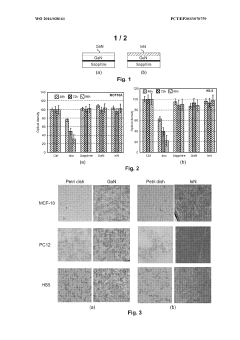
- An implantable electrode made of Indium nitride (InN) is used, which is electrically conductive, inhibits cell adhesion, and exhibits low toxicity, reducing bio-fouling and enhancing signal quality by preventing cell growth on its surface, thus improving the signal-to-noise ratio and extending the electrode's longevity.
Micro-devices for disease detection
PatentActiveUS20180088068A1
Innovation
- Development of innovative micro-devices integrated with advanced fabrication technologies for disease detection at microscopic levels, capable of measuring various biological properties with high sensitivity and specificity, using techniques such as micro-electro-mechanical systems (MEMS) and integrated circuit fabrication to create sophisticated disease detection apparatus.


Biocompatibility and Safety Considerations
Biocompatibility remains a paramount concern in the development of semiconductor materials for bioelectronic interfaces. When these materials come into direct contact with biological tissues, they must not elicit adverse immune responses, inflammation, or cytotoxicity. Silicon-based materials have demonstrated relatively good biocompatibility in short-term applications, though long-term implantation can lead to encapsulation by fibrous tissue, potentially degrading device performance. In contrast, gallium nitride (GaN) has shown exceptional biocompatibility profiles in recent studies, with minimal inflammatory responses observed in both in vitro and in vivo models.
Carbon-based semiconductors, particularly graphene and diamond-like carbon, exhibit excellent biocompatibility due to their chemical inertness and structural similarity to biological carbon compounds. These materials have demonstrated minimal protein adsorption and cellular adhesion, reducing the risk of biofouling that commonly plagues implanted devices. However, the manufacturing processes for these materials often involve potentially toxic precursors, necessitating rigorous purification protocols.
The degradation behavior of semiconductor materials in physiological environments presents significant safety considerations. Silicon gradually degrades in biological fluids, potentially releasing silicon particles that may trigger inflammatory responses. Organic semiconductors, while offering flexibility advantages, can degrade more rapidly, potentially releasing byproducts with unknown toxicological profiles. This degradation not only raises safety concerns but also impacts device longevity and reliability in clinical applications.
Surface modification strategies have emerged as critical approaches to enhance biocompatibility while maintaining semiconductor functionality. Techniques such as polymer coating, biomolecule functionalization, and nanopatterning can significantly improve the biological interface without compromising electrical performance. For instance, polyethylene glycol (PEG) coatings on silicon surfaces have been shown to reduce protein adsorption and subsequent inflammatory responses, while maintaining charge carrier mobility.
Regulatory considerations for semiconductor materials in bioelectronic interfaces have become increasingly stringent. Materials must undergo comprehensive biocompatibility testing according to ISO 10993 standards, including cytotoxicity, sensitization, and genotoxicity assessments. Additionally, leachable compounds and degradation products require thorough characterization and toxicological evaluation. The FDA and equivalent regulatory bodies worldwide have established specific guidance for implantable electronic devices, with particular emphasis on long-term safety profiles and potential systemic effects.
Emerging semiconductor materials such as indium gallium zinc oxide (IGZO) and molybdenum disulfide (MoS2) show promising biocompatibility profiles in preliminary studies, but require more extensive in vivo evaluation before clinical translation. The biocompatibility assessment must also consider the entire device ecosystem, including packaging materials, interconnects, and encapsulation layers, as these components equally influence the overall biological response to implanted bioelectronic interfaces.
Regulatory Framework for Implantable Bioelectronic Devices
The regulatory landscape for implantable bioelectronic devices incorporating semiconductor materials presents a complex framework that varies significantly across global jurisdictions. In the United States, the Food and Drug Administration (FDA) classifies these devices primarily under Class III, requiring rigorous premarket approval (PMA) processes that specifically evaluate the biocompatibility of semiconductor materials like silicon, gallium arsenide, and graphene when interfacing with biological tissues.
The European Union's Medical Device Regulation (MDR) and In Vitro Diagnostic Regulation (IVDR) implement more stringent requirements for bioelectronic implants, particularly emphasizing long-term safety assessments for novel semiconductor materials. The MDR specifically addresses the unique challenges posed by different semiconductor materials, requiring manufacturers to demonstrate material stability under physiological conditions and provide comprehensive biocompatibility data.
Japan's Pharmaceuticals and Medical Devices Agency (PMDA) has established specialized evaluation pathways for bioelectronic interfaces, with particular attention to semiconductor degradation patterns and potential leaching of compounds in the biological environment. Their framework includes specific provisions for silicon-based versus compound semiconductor materials in implantable applications.
International standards such as ISO 10993 series for biological evaluation of medical devices and IEC 60601 for electrical medical equipment safety provide critical benchmarks for semiconductor material selection in bioelectronic interfaces. These standards are continuously evolving to address emerging semiconductor technologies, with recent updates specifically addressing nanomaterials and two-dimensional semiconductors.
Regulatory bodies increasingly require post-market surveillance specific to semiconductor material performance, recognizing that laboratory testing may not fully predict long-term in vivo behavior. This includes monitoring for semiconductor degradation, potential toxicity from breakdown products, and changes in electrical characteristics over time.
The regulatory pathway complexity varies significantly based on the specific semiconductor material employed. Silicon-based devices generally face more established regulatory pathways, while novel materials like graphene, molybdenum disulfide, or organic semiconductors encounter more extensive testing requirements due to limited clinical history. Manufacturers must navigate material-specific regulatory considerations that evaluate both electrical performance and biological safety profiles.
Harmonization efforts are underway through initiatives like the International Medical Device Regulators Forum (IMDRF) to standardize evaluation criteria for semiconductor materials in bioelectronic interfaces, though significant regional differences persist. These efforts aim to establish consistent safety and performance standards while accelerating approval processes for innovative semiconductor technologies in medical applications.
Unlock deeper insights with Patsnap Eureka Quick Research — get a full tech report to explore trends and direct your research. Try now!
Generate Your Research Report Instantly with AI Agent
Supercharge your innovation with Patsnap Eureka AI Agent Platform!