The Role of Nanostructures in Bioelectronic Interface Efficiency
OCT 15, 202510 MIN READ
Generate Your Research Report Instantly with AI Agent
Patsnap Eureka helps you evaluate technical feasibility & market potential.
Nanostructure Bioelectronics Background and Objectives
Bioelectronic interfaces represent a critical intersection between biological systems and electronic devices, enabling unprecedented capabilities in healthcare monitoring, neural interfaces, and therapeutic applications. The evolution of this field has been marked by significant technological advancements, particularly in the last two decades, with nanostructures emerging as transformative elements that fundamentally enhance interface efficiency.
The historical trajectory of bioelectronic interfaces began with rudimentary metal electrodes in the mid-20th century, progressing through microfabrication techniques in the 1980s-1990s, and ultimately embracing nanotechnology in the early 2000s. This progression has been driven by the persistent challenges of achieving stable, long-term connections between biological tissues and electronic components while minimizing immune responses and signal degradation.
Nanostructures—including nanowires, nanotubes, graphene, and other nanoscale materials—have revolutionized this field by offering unique properties that address fundamental limitations. Their high surface-to-volume ratio significantly improves signal transduction, while their dimensional compatibility with cellular structures enables more intimate integration with biological systems at the molecular level.
The current technological momentum is directed toward developing bioelectronic interfaces that can seamlessly integrate with living tissues, providing high-fidelity, bidirectional communication between biological and electronic systems. This integration aims to enable precise monitoring of physiological parameters and targeted modulation of biological functions with minimal invasiveness and maximum biocompatibility.
Key technological objectives in this domain include enhancing signal-to-noise ratios, reducing interface impedance, improving long-term stability in physiological environments, minimizing foreign body responses, and developing self-powered or wirelessly powered systems. Additionally, there is significant focus on creating flexible, stretchable interfaces that can accommodate the dynamic nature of biological tissues.
The convergence of nanotechnology with bioelectronics has opened new frontiers in neural prosthetics, brain-machine interfaces, advanced biosensors, and targeted drug delivery systems. These applications hold transformative potential for treating neurological disorders, enabling advanced prosthetics with sensory feedback, and developing next-generation implantable medical devices.
Looking forward, the field is trending toward increasingly sophisticated nanostructured interfaces that incorporate biomimetic designs, self-assembly capabilities, and responsive functionalities. These advances aim to create truly symbiotic relationships between electronic systems and biological hosts, potentially enabling revolutionary applications in regenerative medicine, neural engineering, and personalized healthcare monitoring.
Market Analysis for Bioelectronic Interfaces
The bioelectronic interfaces market is experiencing robust growth, driven by increasing applications in healthcare, neuroscience, and biomedical engineering. Current market valuations indicate that the global bioelectronic medicine sector reached approximately $17.5 billion in 2022 and is projected to grow at a compound annual growth rate (CAGR) of 11.4% through 2030. Nanostructured interfaces represent a significant segment within this market, with specialized applications commanding premium pricing due to their enhanced performance characteristics.
Demand for high-efficiency bioelectronic interfaces is particularly strong in neural implants, biosensors, and advanced prosthetics. The neural interface segment alone is expected to reach $3.3 billion by 2027, with nanostructured interfaces accounting for an increasing share of this value. Healthcare providers and research institutions constitute the primary customer base, with pharmaceutical companies and defense agencies emerging as secondary markets with substantial purchasing power.
Regional analysis reveals North America currently dominates the market with approximately 42% share, followed by Europe (28%) and Asia-Pacific (22%). However, the Asia-Pacific region is demonstrating the fastest growth rate at 13.7% annually, primarily driven by increased research funding in China, Japan, and South Korea. Emerging economies are showing heightened interest in cost-effective nanostructured solutions that can address their specific healthcare challenges.
Key market drivers include the aging global population, rising prevalence of neurological disorders, and increasing investment in bioelectronic medicine research. The convergence of nanotechnology with bioelectronics has created a distinct high-value market segment where interface efficiency directly correlates with commercial success. Consumer demand for minimally invasive medical technologies and personalized healthcare solutions further accelerates market expansion.
Market barriers include stringent regulatory requirements, particularly for implantable devices, which extend development timelines and increase costs. The average approval process for novel bioelectronic interfaces incorporating nanostructures takes 3-5 years in major markets. Additionally, reimbursement challenges and high initial production costs limit widespread adoption despite proven clinical benefits.
Industry forecasts suggest that nanostructured bioelectronic interfaces will experience accelerated commercialization between 2025-2030 as manufacturing processes mature and economies of scale reduce production costs. The market is transitioning from primarily research-focused applications toward clinical implementation, with several breakthrough products expected to receive regulatory approval within the next 36 months. This shift will likely trigger market consolidation as established medical device manufacturers acquire innovative startups with promising nanostructure technologies.
Current Nanostructure Technologies and Barriers
The current landscape of nanostructure technologies for bioelectronic interfaces presents a diverse array of innovative approaches. Carbon-based nanomaterials, particularly carbon nanotubes (CNTs) and graphene, have emerged as leading candidates due to their exceptional electrical conductivity, mechanical flexibility, and biocompatibility. These materials facilitate efficient signal transduction between biological systems and electronic devices, with CNTs demonstrating capability to detect single-molecule events in neural interfaces.
Metal-based nanostructures, including gold nanorods and silver nanowires, offer plasmonic properties that enhance signal detection sensitivity. These structures have been successfully implemented in biosensing applications, achieving detection limits in the femtomolar range. Silicon nanowires and nanopillars represent another significant category, providing high surface-to-volume ratios that maximize the interface area with biological entities while maintaining minimal invasiveness.
Polymer-based nanostructures have gained traction for their tunable properties and ease of functionalization. Materials such as PEDOT:PSS (poly(3,4-ethylenedioxythiophene) polystyrene sulfonate) demonstrate remarkable charge transfer capabilities while maintaining softness that reduces mechanical mismatch with biological tissues. Recent advances in conducting polymer nanofibers have shown promise in long-term neural recording applications.
Despite these technological achievements, significant barriers impede widespread implementation. Biocompatibility remains a primary concern, as many nanomaterials trigger inflammatory responses or exhibit cytotoxicity during long-term implantation. The foreign body response often leads to encapsulation of devices by scar tissue, degrading signal quality over time. This challenge is particularly pronounced in neural interfaces where stable recordings are essential for clinical applications.
Manufacturing scalability presents another substantial hurdle. Many cutting-edge nanostructures require complex fabrication processes that are difficult to standardize and scale for commercial production. Techniques such as electron beam lithography offer precise control but remain prohibitively expensive and time-consuming for mass production. Alternative approaches like self-assembly methods show promise but struggle with reproducibility issues.
Signal stability and longevity constitute persistent challenges, with many nanostructure-based interfaces experiencing performance degradation within weeks or months of implantation. This limitation stems from material degradation in biological environments, electrode fouling by protein adsorption, and shifting tissue-electrode interfaces due to micromotion. Recent efforts to address these issues include development of anti-fouling coatings and flexible substrate materials that move with tissue.
Regulatory hurdles further complicate translation to clinical applications, as novel nanomaterials face extensive safety testing requirements and unclear regulatory pathways. The complexity of these materials often necessitates new evaluation frameworks beyond traditional medical device assessments.
Existing Nanostructure Solutions for Biointerfaces
01 Nanostructured interfaces for improved energy conversion
Nanostructured interfaces can significantly enhance energy conversion efficiency in various applications. By engineering the interface at the nanoscale, electron transfer and charge separation can be optimized, reducing recombination losses. These interfaces typically feature controlled morphology and composition to facilitate efficient charge transport across boundaries. The implementation of such nanostructures has shown substantial improvements in photovoltaic devices, fuel cells, and other energy conversion systems.- Nanostructured interfaces for improved energy conversion: Nanostructured interfaces can significantly enhance energy conversion efficiency in various applications. By engineering the interface between different materials at the nanoscale, electron transfer and charge separation can be optimized. These interfaces reduce recombination losses and improve charge carrier mobility, leading to higher overall efficiency in solar cells, photocatalysts, and other energy conversion devices. The controlled architecture of these interfaces allows for better light absorption and utilization across broader spectral ranges.
- Surface modification of nanostructures for enhanced interface properties: Surface modification techniques can be applied to nanostructures to enhance their interface properties. These modifications include functionalization with specific chemical groups, coating with thin films, or creating core-shell structures. Such treatments can improve compatibility between nanostructures and surrounding matrices, enhance wettability, reduce interfacial resistance, and prevent aggregation. These modifications are crucial for applications requiring efficient charge or energy transfer across interfaces, such as in electronic devices, sensors, and catalytic systems.
- Nanostructured interfaces for electronic and optoelectronic applications: Nanostructured interfaces play a critical role in electronic and optoelectronic devices by facilitating efficient charge transport and light manipulation. These interfaces can be engineered to control band alignment, reduce contact resistance, and enhance carrier injection or extraction. By incorporating quantum dots, nanowires, or two-dimensional materials at interfaces, device performance metrics such as conductivity, switching speed, and quantum efficiency can be significantly improved. Applications include high-performance transistors, light-emitting diodes, photodetectors, and memory devices.
- Biomimetic and bioinspired nanostructured interfaces: Biomimetic and bioinspired approaches to designing nanostructured interfaces leverage natural principles to achieve enhanced efficiency. These interfaces mimic structures found in biological systems, such as hierarchical arrangements in plant leaves or moth eyes, to create surfaces with special properties like self-cleaning, anti-reflection, or selective permeability. The resulting nanostructured interfaces demonstrate improved energy transfer, reduced biofouling, enhanced catalytic activity, and better biocompatibility, making them valuable for applications in medicine, environmental remediation, and sustainable energy systems.
- Fabrication methods for high-efficiency nanostructured interfaces: Advanced fabrication techniques are essential for creating high-efficiency nanostructured interfaces with precise control over morphology and composition. These methods include template-assisted growth, atomic layer deposition, self-assembly processes, and lithographic techniques. Each approach offers specific advantages for controlling interface properties such as roughness, porosity, crystallinity, and chemical composition. Novel processing methods enable the creation of complex hierarchical structures with tailored interfaces that maximize efficiency in applications ranging from catalysis and sensing to energy storage and conversion.
02 Surface modification of nanostructures for enhanced interface properties
Surface modification techniques can be applied to nanostructures to enhance their interface properties. These modifications include functionalization with specific chemical groups, coating with thin films, or creating core-shell structures. Such treatments can improve compatibility between different materials, enhance binding to substrates, and optimize electronic properties at interfaces. Modified nanostructure surfaces show improved wettability, adhesion, and electrical contact, leading to higher overall system efficiency.Expand Specific Solutions03 Nanoscale interface engineering for optical applications
Engineering nanoscale interfaces can dramatically improve optical device performance. By controlling the interface structure at the nanometer scale, light absorption, emission, and propagation can be optimized. These engineered interfaces can reduce reflection losses, enhance light trapping, and improve quantum efficiency in photodetectors and light-emitting devices. Techniques such as creating gradient index interfaces, plasmonic structures, and photonic crystals at interfaces have demonstrated significant improvements in optical device efficiency.Expand Specific Solutions04 Nanostructured interfaces for thermal management and heat transfer
Nanostructured interfaces can significantly enhance thermal management and heat transfer efficiency. By engineering interface morphology at the nanoscale, thermal boundary resistance can be reduced while thermal conductivity is increased. These interfaces often incorporate specific patterns, hierarchical structures, or composite materials to optimize phonon transport across boundaries. Applications include improved heat dissipation in electronic devices, enhanced thermal barrier coatings, and more efficient heat exchangers.Expand Specific Solutions05 Fabrication methods for high-efficiency nanostructured interfaces
Advanced fabrication techniques are essential for creating high-efficiency nanostructured interfaces. These methods include atomic layer deposition, template-assisted growth, self-assembly processes, and precision etching techniques. Such approaches enable precise control over interface composition, geometry, and crystallinity at the nanoscale. The development of scalable and reproducible fabrication methods is crucial for implementing nanostructured interfaces in commercial applications while maintaining their performance advantages.Expand Specific Solutions
Leading Organizations in Nanostructure Bioelectronics
The nanostructure bioelectronic interface market is currently in a growth phase, characterized by increasing research activity and early commercialization efforts. The global bioelectronics market is projected to reach approximately $25 billion by 2025, with nanostructured interfaces representing a rapidly expanding segment. Technologically, the field remains in early-to-mid maturity, with significant advancements being made by academic institutions like University of California, University of Copenhagen, and Northwestern University collaborating with industry leaders such as IBM and DexCom. Research organizations including CEA and Whitehead Institute are driving fundamental innovations, while companies like GE Healthcare and Agilent Technologies are translating these discoveries into commercial applications. The convergence of nanotechnology expertise from universities and the manufacturing capabilities of corporations is accelerating development, though challenges in biocompatibility, long-term stability, and scalable production persist.
The Regents of the University of California
Technical Solution: The University of California has pioneered nanoscale bioelectronic interfaces through their development of flexible nanoelectrode arrays that can seamlessly integrate with biological tissues. Their technology utilizes ultra-thin nanowire structures with diameters below 100 nm to create high-density electrode arrays capable of single-cell resolution recording. These arrays incorporate specialized surface modifications with biocompatible materials like PEDOT:PSS and graphene to reduce electrode impedance and enhance signal quality. UC researchers have demonstrated long-term stability in vivo with minimal foreign body response through their proprietary stealth coating technology that mimics cell membrane structures. Their recent innovations include wireless power transfer systems specifically designed for implantable nanoelectronic interfaces, enabling continuous monitoring without external wiring constraints.
Strengths: Superior biocompatibility through biomimetic surface engineering; exceptional spatial resolution for single-cell recording; demonstrated long-term stability in chronic implantation studies. Weaknesses: Manufacturing scalability challenges for high-density arrays; higher production costs compared to conventional microelectrodes; limited power efficiency in wireless implementations.
International Business Machines Corp.
Technical Solution: IBM has developed advanced nanostructured bioelectronic interfaces leveraging their expertise in semiconductor fabrication and materials science. Their proprietary technology employs nanoporous silicon structures with precisely controlled pore sizes (5-20 nm) to create high surface area electrodes that significantly enhance signal transduction at the bio-electronic interface. IBM's approach incorporates atomically precise carbon nanotube arrays functionalized with specific biomolecules to achieve selective detection of biomarkers at femtomolar concentrations. Their platform integrates on-chip signal processing using neuromorphic computing architectures that mimic biological neural networks, enabling real-time data analysis with minimal power consumption. IBM has demonstrated practical applications in continuous glucose monitoring systems with response times under 1 second and drift rates below 2% over 30 days, representing significant improvements over conventional technologies.
Strengths: Exceptional manufacturing precision and scalability leveraging semiconductor fabrication expertise; superior signal-to-noise ratio through nanoscale engineering; integrated computing capabilities for real-time signal processing. Weaknesses: Higher initial development costs; complex integration requirements with existing medical device ecosystems; potential regulatory hurdles for novel nanomaterials.
Key Patents in Bioelectronic Interface Efficiency
Customizable and renewable nanostructured interface for bioelectronic applications
PatentInactiveUS8435773B2
Innovation
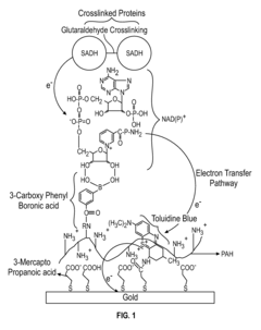
- A biomimetic device with a polyelectrolyte-bound enzyme system that allows reversible binding to a treated substrate electrode, facilitating efficient electron transfer and regeneration by electrostatic attraction, using charged polyelectrolytes like poly(allylamine hydrochloride) and poly(ethyleneimine) to maintain the enzyme, cofactor, and mediator in proper orientation, enabling efficient electron transfer and easy regeneration.
Method to impose a geometric arrangement to binding partners present on a biological interface
PatentWO2025125524A1
Innovation
- The method involves using planar rigid nanostructures with specific geometric arrangements of binding units, restricting the spatial freedom of binding partners and enhancing the precision and selectivity of interactions by imposing a defined spatial framework.
Biocompatibility and Safety Considerations
The integration of nanostructures with biological systems presents significant biocompatibility and safety challenges that must be addressed before widespread clinical application. Nanomaterials used in bioelectronic interfaces, including carbon nanotubes, graphene, gold nanoparticles, and silicon nanowires, each exhibit unique interactions with biological tissues that can trigger immune responses, inflammation, or cytotoxicity if not properly engineered.
Surface chemistry plays a crucial role in determining biocompatibility. Functionalization of nanostructures with biocompatible coatings such as polyethylene glycol (PEG), phospholipids, or specific proteins can significantly reduce adverse biological reactions while maintaining electrical conductivity. Recent studies have demonstrated that biomimetic approaches, where nanostructures are designed to resemble natural cellular components, show promising improvements in long-term tissue integration and reduced foreign body responses.
Cytotoxicity assessment protocols for nanomaterials in bioelectronic interfaces have evolved substantially, with standardized in vitro and in vivo testing methodologies now available. These include cell viability assays, inflammatory marker analyses, and histopathological evaluations following implantation. Emerging evidence suggests that nanostructure geometry, aspect ratio, and surface charge density are critical determinants of cellular toxicity, with smaller dimensions often associated with greater potential for cellular internalization and subsequent damage.
Long-term stability represents another significant challenge, as degradation of nanomaterials in the biological environment may release potentially toxic components. Studies tracking the fate of implanted nanostructures have revealed that certain materials undergo gradual dissolution, while others may persist indefinitely. This variability necessitates material-specific safety profiles and degradation kinetics understanding for each bioelectronic application.
Regulatory frameworks for nanostructure-based bioelectronic interfaces remain under development globally. The FDA and EMA have established preliminary guidelines for nanomaterial safety assessment, though these continue to evolve as new scientific evidence emerges. Current approaches typically require comprehensive characterization of physicochemical properties, biodistribution studies, and long-term toxicological evaluations before clinical translation.
Risk mitigation strategies include encapsulation technologies that isolate potentially harmful nanomaterials while maintaining their functional properties. Advanced imaging techniques such as intravital microscopy now enable real-time monitoring of nanostructure-tissue interactions, providing valuable insights for safety optimization. Additionally, computational modeling approaches are increasingly employed to predict potential toxicological outcomes based on nanomaterial properties, accelerating the screening process for biocompatible candidates.
Scalability and Manufacturing Challenges
The scaling of nanostructured bioelectronic interfaces from laboratory prototypes to commercial products presents significant manufacturing challenges. Current fabrication methods for high-performance bioelectronic interfaces often rely on sophisticated cleanroom techniques such as electron beam lithography and focused ion beam milling, which are inherently low-throughput and high-cost. These limitations create substantial barriers to widespread adoption and commercialization of advanced bioelectronic devices.
Material consistency represents another critical challenge in scaling nanostructured interfaces. The performance of bioelectronic interfaces depends heavily on precise control of nanoscale features, where even minor variations can significantly impact electrical properties and biocompatibility. Maintaining this precision across large-scale production runs requires advanced process control systems and quality assurance protocols that are still evolving for nanomaterials.
The integration of multiple materials and components at the nanoscale introduces additional complexity to manufacturing workflows. Many cutting-edge bioelectronic interfaces combine organic semiconductors, metallic nanostructures, and biological components in hierarchical architectures. Each material system requires specific handling protocols, and their integration demands carefully orchestrated manufacturing sequences that preserve the functional properties of each component.
Cost considerations further complicate the scalability equation. While laboratory-scale production can justify expensive materials and processes for proof-of-concept demonstrations, commercial viability demands substantial cost reductions. The economic feasibility of scaled production depends on identifying alternative materials and developing more efficient fabrication routes that maintain performance while reducing per-unit costs.
Regulatory compliance adds another dimension to manufacturing challenges. Bioelectronic interfaces intended for medical applications must meet stringent safety and reliability standards. The novel materials and structures that enable enhanced performance at the bioelectronic interface often lack established safety profiles, necessitating extensive testing and validation before regulatory approval can be secured.
Recent advances in roll-to-roll processing, nanoimprint lithography, and directed self-assembly offer promising pathways toward more scalable manufacturing. These approaches enable parallel fabrication of nanostructured surfaces across larger areas than traditional methods allow. However, significant research investment is still required to adapt these techniques for the specific requirements of bioelectronic interfaces, particularly for applications demanding precise control over both electronic and biological functionalities.
Unlock deeper insights with Patsnap Eureka Quick Research — get a full tech report to explore trends and direct your research. Try now!
Generate Your Research Report Instantly with AI Agent
Supercharge your innovation with Patsnap Eureka AI Agent Platform!
